hesam.moshiri
A. Circuit Analysis
Figure 1 shows the schematic diagram of the device. As it is clear, the circuit consists of 3 main parts: Arduino-Nano (Controller), FM receiver module, and the audio amplifier.

Figure 1, Schematic diagram of the digital FM receiver
A-1. FM Receiver Module
The FM receiver module is based on the TEA5767 [1, 2] chip. It is a well-known module that could be controlled via the I2C bus. It covers the FM frequency range from 76MHz to 108MHz. At the output, it handles L and R stereo audio signals that should be amplified, otherwise, the sound level is weak and can not be heard even by an earphone. The frequency selection and signal-strength measurement tasks are performed by the Arduino-Nano code.
R3, C7, C8, and C9 build a first-order low pass RC filter that reduces the supply noise. R1 and R2 are mandatory pull-up resistors for the I2C bus and CON1 is a UFL connector that provides an antenna connection. Figure 2 shows the TEA5767 module.
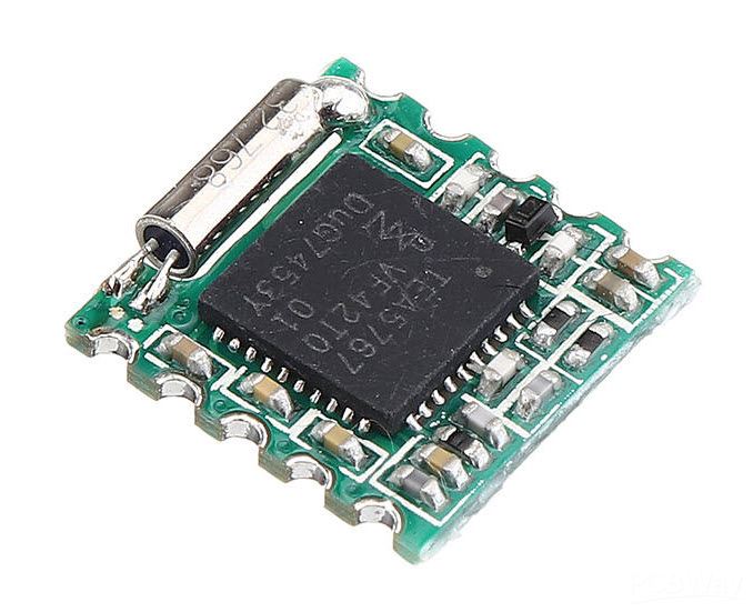
Figure 2, The TEA5767 FM receiver module
A.2 Audio Amplifier
The audio amplifier part consists of the PAM8403 [3, 4] chip. This chip is a 3W+3W HiFi Class-D amplifier that can operate with only a single 5V supply. The maximum output power can be achieved using 4-ohm speakers. According to the datasheet: “The PAM8403 is a 3W, class-D audio amplifier. It offers low THD+N, allowing it to achieve high-quality sound reproduction. The new filterless architecture allows the device to drive the speaker directly, requiring no low-pass output filters, thus saving the system costs and PCB area”.
C13, C14, and C15 are bypass capacitors that are used to reduce the supply noise. R4, R5, C11, and C12 are used to transfer the output audio to the amplifier. Figure 3 shows the reference circuit of the PAM8403 chip. P2 and P3 are right-angle 2-pin XH connectors that are used to connect the speakers to the board.

Figure 3, Datasheet reference circuit of the PAM8403
A.3 Controller
The controller of the circuit consists of an Arduino-Nano board (AR1). Figure 4 shows the Arduino-Nano board. The board drives an 8*2 LCD (LCD1) and also reads the status of the SW1, SW2, and SW3 push buttons. It also sends/receives the TEA5767 data through the I2C bus. R6 sets the contrast level of the LCD and C4, C5, and C6 are used to reduce the mechanical push-button noises (debouncing).

Figure 4, The Arduino-Nano board
A.4 Power Supply
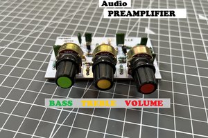
The TS2937 [5, 6] is the main component of the power supply that provides a stable +5V supply for the circuit. C1, C2, and C3 are used to reduce the noise, and POT1 is a 50K 2-way (dual) potentiometer with a switch. The POT1 both turns ON/OFF the device and increases or decreases the sound level. Picture 5 shows a picture of the POT1.

Figure 5, 2-Way (Dual) potentiometer with Switch
B. PCB Layout
Figure 6 shows the PCB layout of the digital FM receiver. It is a 2 layers PCB board, last revision. The Arduino-Nano board is mounted on the bottom side and LCD on the top side of the board, preferably on female pin headers. This is more clear in 3D views and real photos. Figure 7 shows the 3D views of the board. Figure 8 shows the high-quality fabricated PCB boards of the digital FM receiver circuit.

Figure 6, The PCB layout of the digital FM receiver

Figure 7, The top and bottom 3D views of the PCB board

Figure 8, High quality fabricated PCB boards
I used the SamacSys component libraries (for IC1 and IC2) in this PCB project as usual. It saves a lot of time and prevents design mistakes which leads to a lower product cost. All SamacSys component libraries (Schematic symbols, PCB footprints, and 3D models) are FREE and they follow strict industrial IPC footprint standards. You can download and install the libraries from the componentsearchengine.com or you can install them directly using the provided CAD plugins. I used the Altium plugin, however, almost all electronic designing CAD software are supported, such as Eagle, KiCad, OrCAD, Proteus...
Read more »
 Xtreme Tech
 Sagar 001