 Mark Atherton
Vector Drawing Machine, Number 3
Background
Being an Engineer, I have always been drawn to the Russian pragmatic method of naming new products. While some idiotic Western Marketeer might name a small CRT based gaming machine ‘The Vectormatic Score-Master 3000’, the Russians tend to use something more meaningful, and since this is attempt three at a vector-based display system, they might call it the Vector Drawing Machine, Number 3. So that is how this project became known as the VDM3. Fifteen–love, Engineering vs Marketing departments.
Many years ago, my imagination was immediately caught with the idea of using a small (oscilloscope) CRT as a method of displaying an analog clock. As well as the possibility of an æsthetically pleasing and gentle display, there is also the utter ridiculousness of such an undertaking. The thought that a small chain of mechanical linkages being replaced with a microprocessor controlling a pair of high voltage differential amplifiers, as well as an independent EHT (is 1000V EHT ?) power supply just to (roughly) tell-the-time is just a bit daft. The whole project was quite a monumental undertaking when one also considers all of the work associated to generate the process steps that end up with a nice looking device, along with the reams of associated design information.
One of the other attractions of this project was the sheer breadth of activities associated with the design. None of the activities were particularly onerous, but taken as a whole, the integration phase of such a project is the usual time to discover any inter-disciplinary weaknesses.
This article is not intended as a construction project, but there may be some design ideas of processes that spark some interest in unexplored, dark alleyways.
Summary
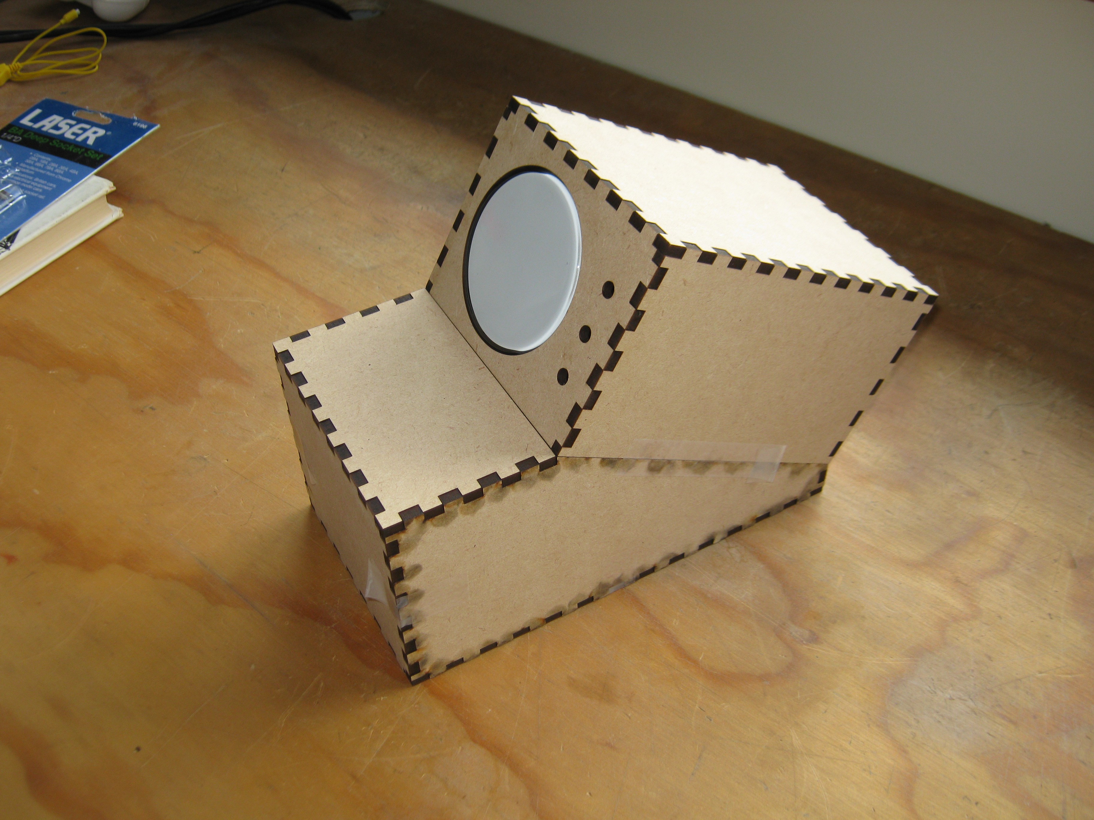
The enclosure is fabricated in two parts using from laser-cut MDF. The top section houses the CRT display readout, HV power supply, deflection and associated controls. The lower section houses joystick, pushbuttons, processor, and low voltage power supply. The rear of the lower section has a DC power socket, as well as a mini-B USB connector. Top and bottom sections slide together. The two are halves are locked together by the Joystick/User Interface panel dropping into place.
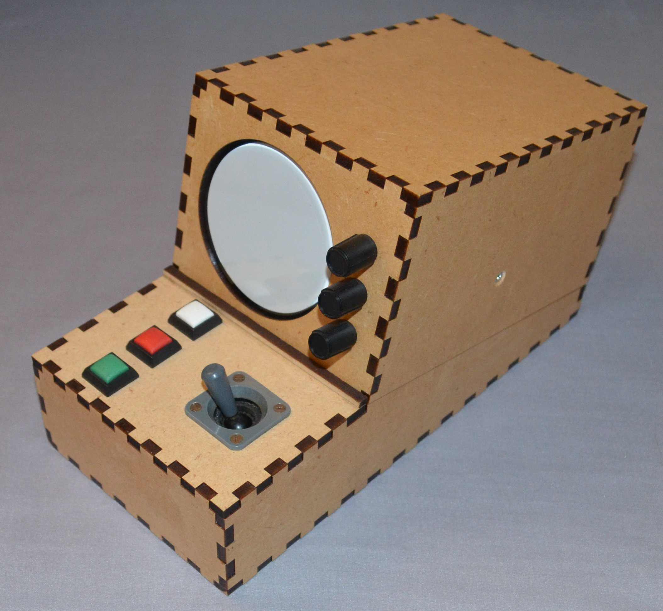
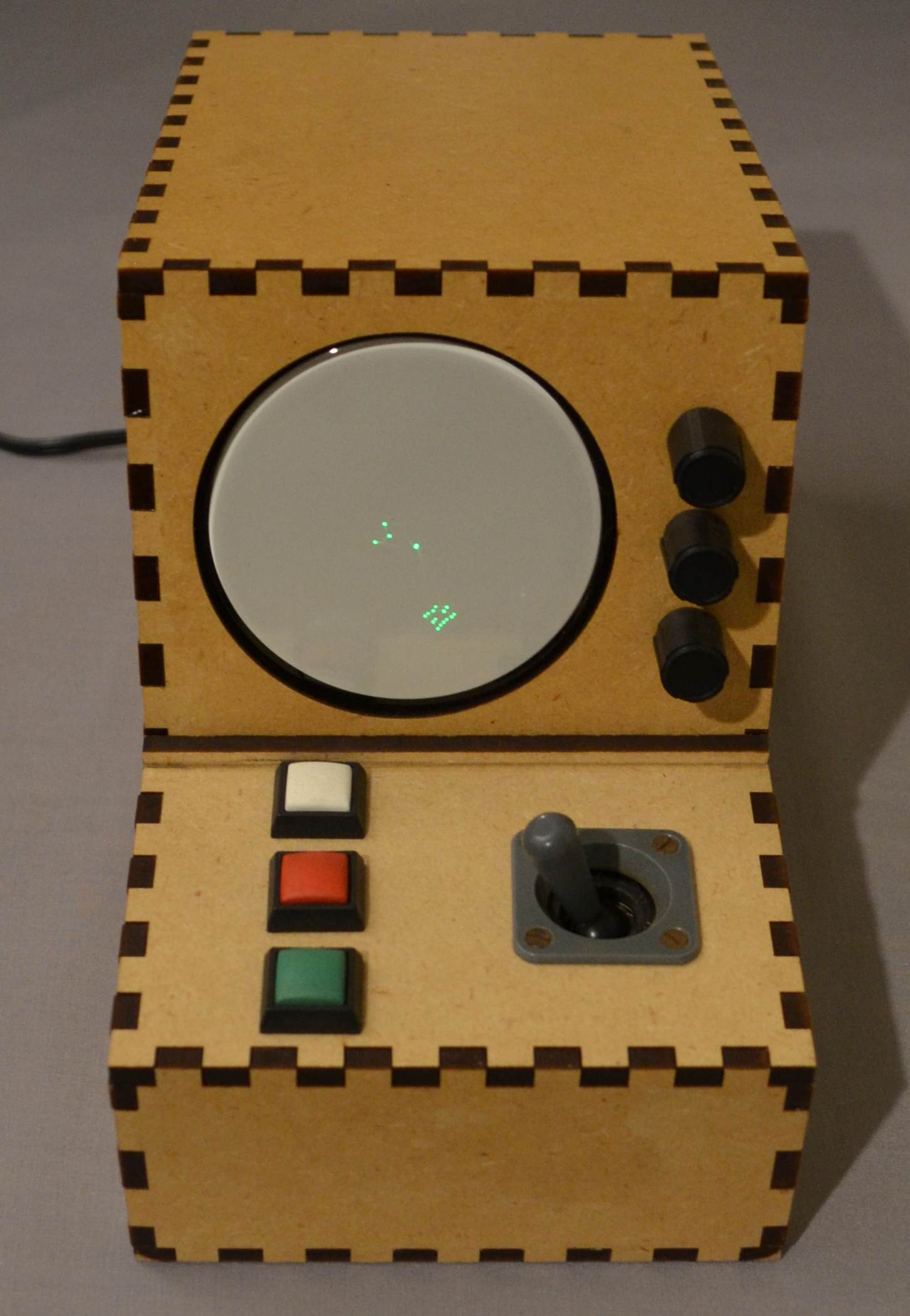
Assembled unit
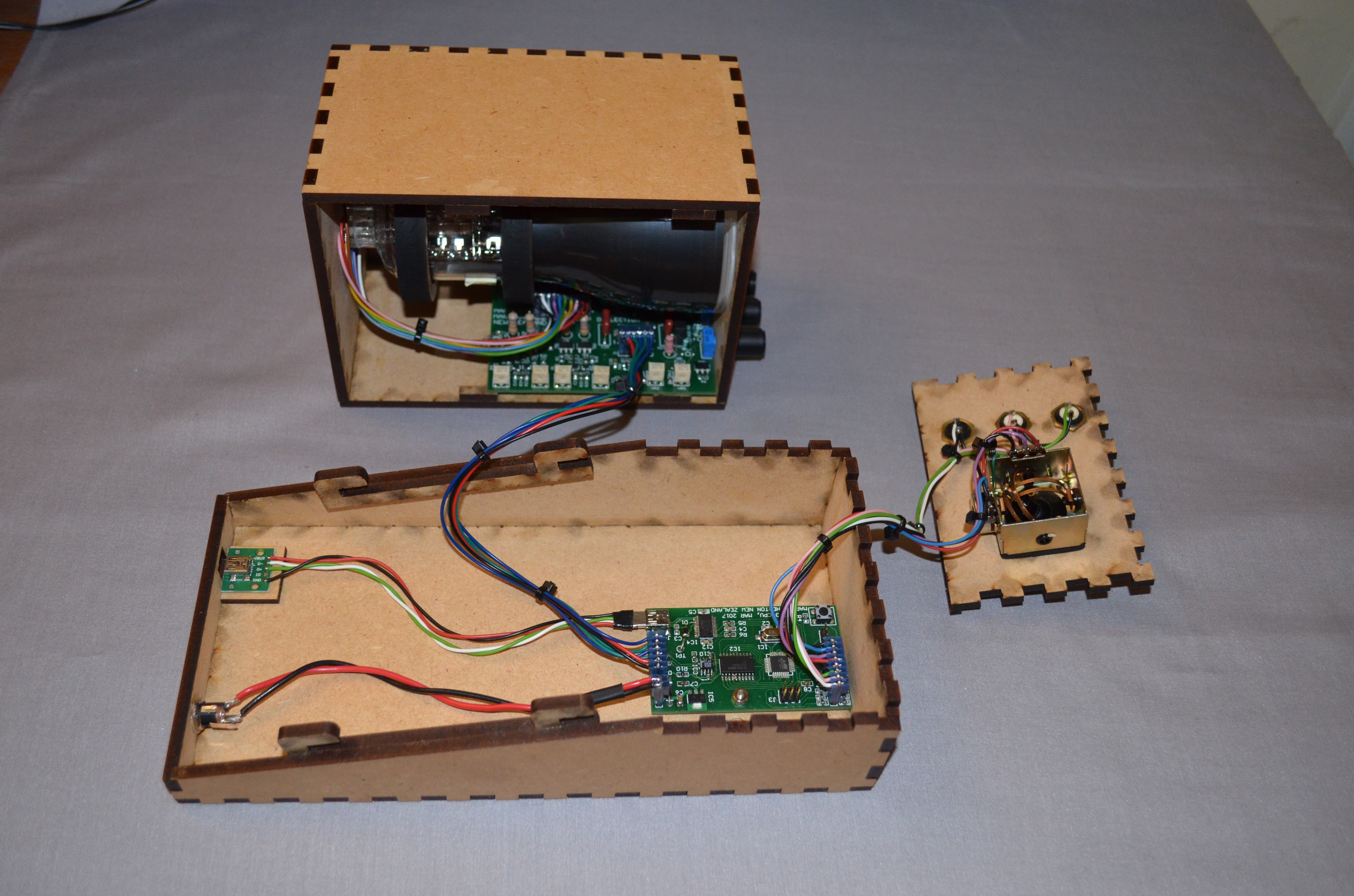
CRT
The CRT is a D7-16G, just over 76mm diameter, 160mm long and designed for battery operation. Three of these CRTs were purchased many years ago for projects such as this one. Base connectors appear to be unavailable.
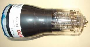
D7-16G CRT
The CRT uses an 11 pin connector, type 30-232 which is not readily available. After a little thought, it appeared that a custom-connector could be fabricated by laser-cutting some acrylic sheet, and reusing suitable valve pin-sockets.
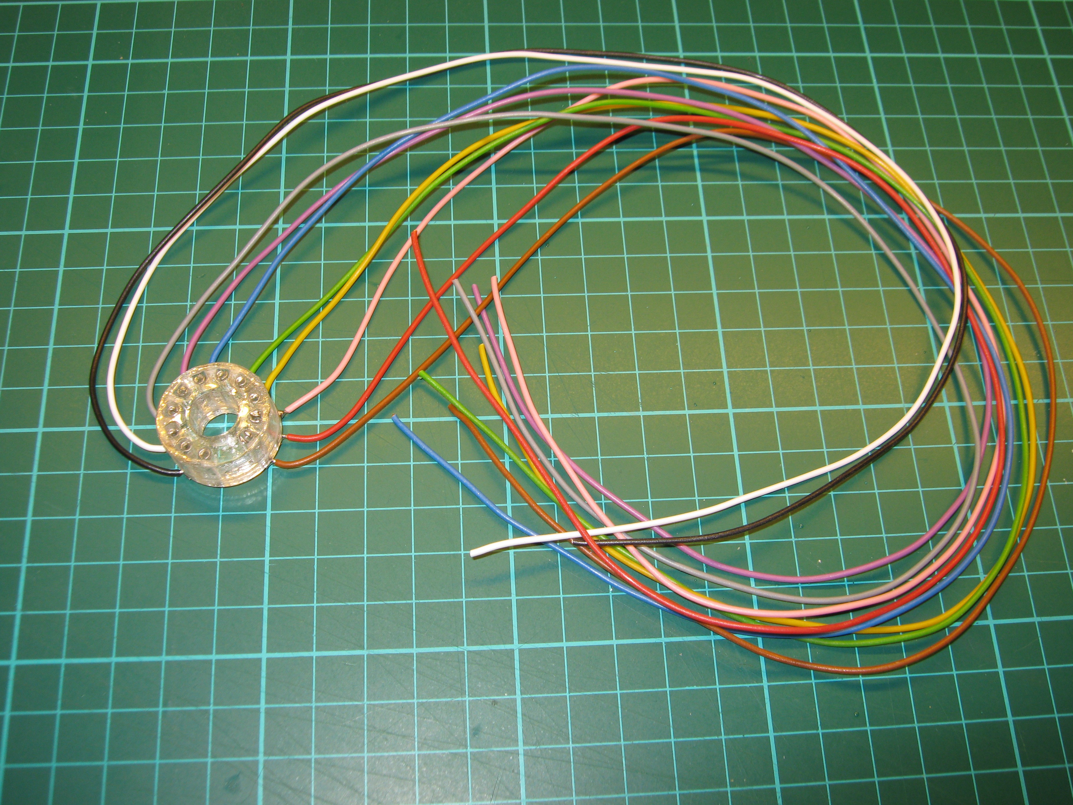
Custom 30-232 CRT connector
Designed using Autosketch, these patterns were created so that the CRT pins were centrally located inside the ‘D’s of the left hand item. Each of these patterns were then cut from 3mm acrylic sheet and glued together. Pin-sockets were removed from a new B9A valve socket, inserted into this new assembly, and bent slightly so that they did not fall out. Flying leads were then soldered and held with heat-shrink sleeving onto each to each pin.
HV PSU
The PSU section is based around an SG3525 switching regulator driving a push-pull pair of N-FETs, and in turn, a small ferrite transformer. The transformer has two secondaries, high and low voltage. The high voltage side passed through a positive half-wave rectifier to generate around 240VDC before being shunt regulated to 210V. This rail delivers around 7mA to the deflection amplifiers. The HV secondary is also voltage doubled to generate around –600V at a milliamp or so to bias the CRT and electron gun. The positive and negative rectifiers are used as an attempt to balance any DC current in the secondary, which may saturate (or at least magnetically bias) the core.
The transformer stack-up starts with primary at the centre. The grounded end of the HV secondary then starts, ending with the hot end of the HV secondary. Finally the LV (heater) winding is wound last. This order was chosen in an attempt to reduce the dielectric stress between the LV winding and the voltage-doubled HV rail. I am having second thoughts about this topology having said this out loud, and will need to investigate the issue at some point.
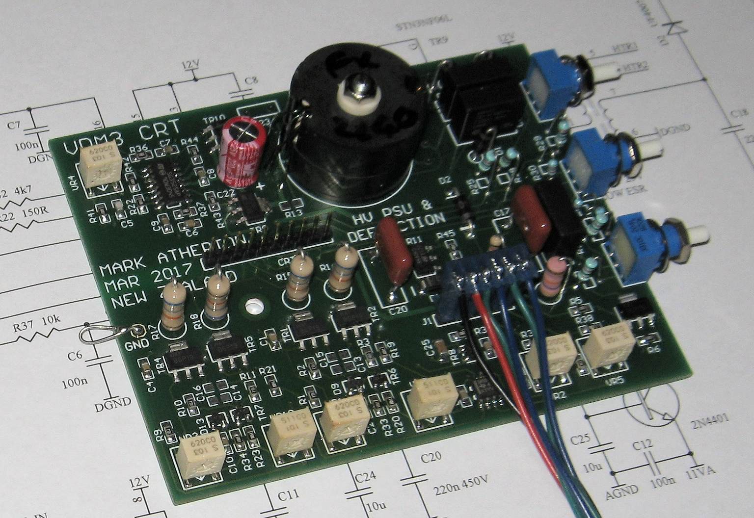
HV and Deflection assembly
It had been a long time since last using a ferrite pot-core, and had completely forgotten that the magnetic material was electrically conductive. This resulted in some HV arcs between the top-end wiring of the secondary and the grounded ferrite. This in turn resulted in failure of several pairs of the STN3NF06L primary side drivers FETs. While the issue was being investigated, these were replaced by a pair of TO252, 100A/8mΩ devices, which are more or less indestructible, even when faced with a 12V, 1A power supply and a shorted-turn transformer to drive.
I was somewhat dismayed to discover that the 3525 switcher was available in wide as well as narrow SOIC packages. The wrong PCB footprint had been used, so single narrow part had to be sourced from the UK at moderate cost.
Deflection amplifier
This sub-system turned out to be quite an interesting beastie to design, so lots of time was spent with a SPICE simulator to understand the issues.
Brief specifications include: Single ended 0..5V input. Differential output with >80V p-p on each limb. Less than 2mA consumption at +210V. +12V power available. No negative power rails available. >500kHz bandwidth, with less than 5o phase-shift over design bandwidth.
Over the course of several days, several topologies were explored, starting with a cascode long-tailed pair with current sink. Initially, only steady state conditions were analysed and optimised. With basic DC performance established, the AC parameters were then explored. The capacitor coupling the emitters of the long tailed-pair (unsurprisingly) significantly affects AC gain, frequency response, and phase performance, and obviously has significant interaction with the emitter resistors, and associated current-sink.
At this point, possible enhancements include thermal stabilisation by thermally-bonding the output devices (given that they are currently SOT-233s, this is not easy). Or of course, changing to a pair of thro-hole devices where this may be achieved more easily.
It would be nice to have a design where shift and gain were less dependant, but an awfully large number of difficult constraints have been satisfied with the current (simple) design, so this extra requirement may just be a bit too onerous.
Processor (and DAC) Board
Given that the main task of the CPU is to re-calculate a string of vector-pairs once every few tens of milliseconds, it seemed reasonable that an inexpensive, but more to the point simple(ish) part would probably be adequate.
Obvious candidates for the job were the Atmel ATmega328P and the ST micro STM32F103C8T6. The former was chosen purely based on complexity, and (at the time) popularity. It was with some surprise during the build of the second set of boards that it was notices that the ‘B’ variants had inadvertently been purchased. More on that later.
The overall CPU board is quite simple, and includes an FT232RL USB bridge, two channel 8-bit voltage DAC, interface to joystick and buttons, optional I2C interface, and a 5V regulator. An Arduino Nano could have been used with a motherboard, but the current solution was chosen for elegance, and wiring simplicity.
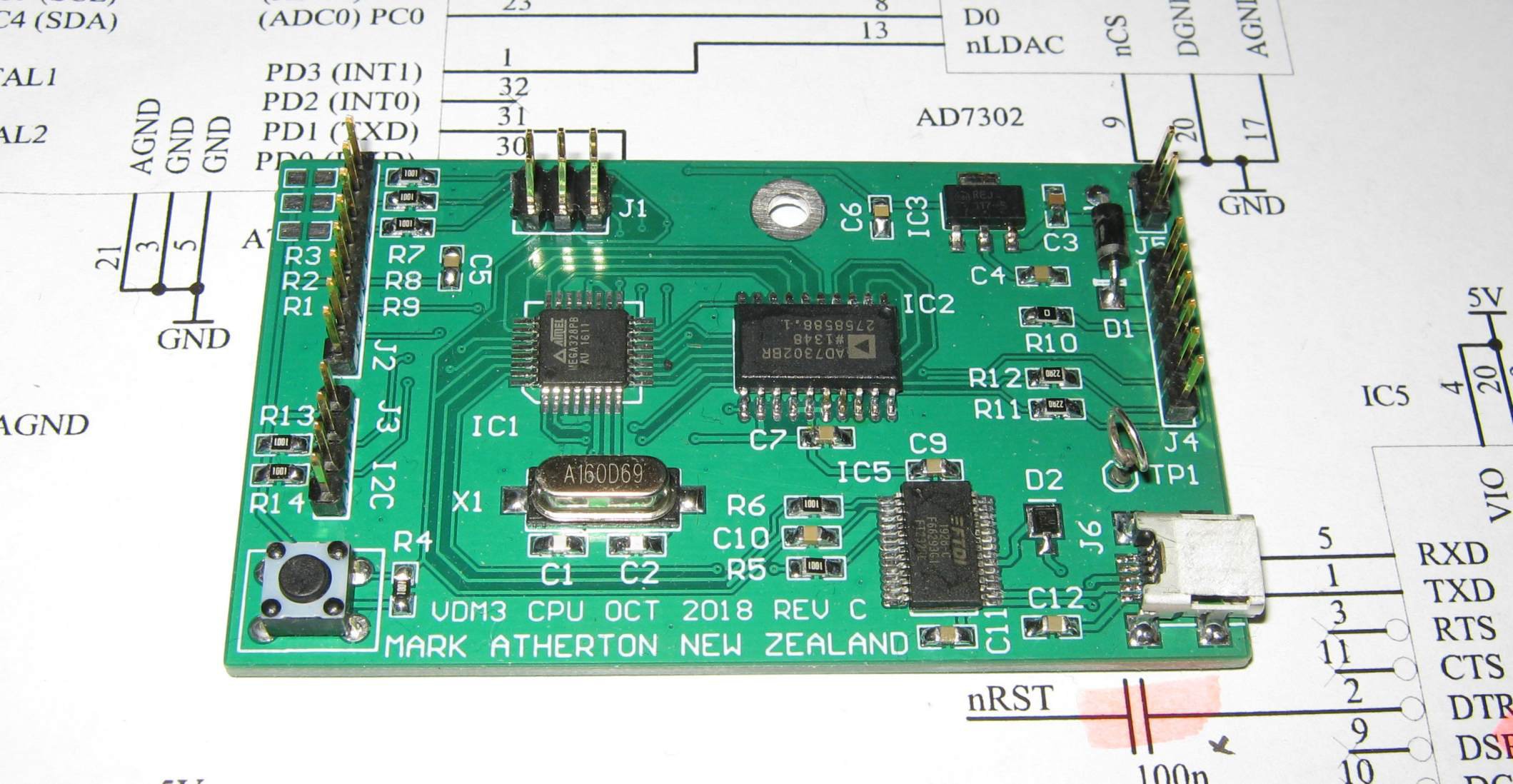
CPU board, with AD7302 DAC
One of the overall system requirements is single-rail operation; this limits available DAC choices. A tube of TLC7528 DACs were available, and at first glance appear to be current DACs, but further reading indicates that they can be configured in voltage mode. In conjunction with the TSH82 op-amps this turned out to be a poor choice, yielding a few percent distortion at signal troughs. The solution to the problems was to change the part to an AD7302, which has a pair of voltage outputs, along with 2us settling time.
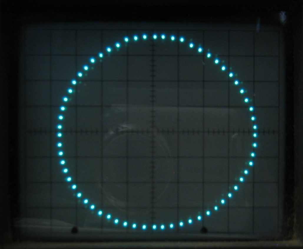
A few percent distortion can ruin your day
In retrospect, there is a chance that the distortion associated with the TLC7528s could be associated with the limited common-mode input range of the associated TSH82 op-amps. This should be easy to test by removing the op-amp, and drawing a lissajous circle on a ‘scope directly using high impedance probes.
Several design flaws pushed the re-fabrication of this apparently simple board: DAC choice, first-use of the FT232RL and omitting to tie the associated TST pin to ground. Also, a mismatch between mini-USB connector schematic and footprint (fixed by making a custom USB extension cable).
New CPU, Toolchain and Bootloader
As I alluded to earlier, it came as somewhat of a surprise to discover that the previously ordered ATmega328Ps were actually the later, and inexplicably less popular ‘B’ variant. This part is binary compatible with its younger brother, all that is except for the chip-signature. The newer part has several useful extra features including a second USART.
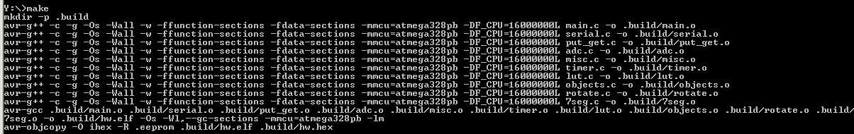
Arduino provided the latest tool-chain, which inexplicably was not available from the Atmel web site. The tools were pulled out and bundled into a portable package, so they no longer were reliant on the Arduino framework. The associated project Makefile was then updated to reference the new CPU and tools.
Given the compatibility of the CPUs, the standard Arduino bootloader was programmed into the new part using AVR studio 4 (which is a relatively small footprint IDE). This was chosen because of its very simple interface. A new chip description XML had to be created from the older version, the main differences being the new part number and associated signature.
Make, and associated makefile are used for firmware development. This approach results in a toolchain approximately of 30MB, rather than the hundreds of megabytes associated with ‘modern’ Integrated Development Environments.
Real programmers don’t use IDEs
Firmware
The system is designed to draw at around 10k vector-pairs per second. For a 50Hz refresh rate, this implies that up to 200 vectors can be displayed. Every 200 vectors (20ms) the foreground is signalled to update the vector list, so that the game may proceed in a reasonably smooth manner.
Vector rotation is required by several processes within the system, and while it is perfectly reasonable to use a decimal value in the range 0..359 degrees, this would require a U16 to be used, which is unnecessarily cumbersome. After a little thought, it seemed reasonable to handle as much data as possible using an S8 (+127 to –128). This is also valid for representing X/Y co-ordinates (given that 8 bit DAC are used) as to represent an angle (approx ±180 degrees).
Screen update is managed through a timer interrupt, and is the only method available to control the DACs. Vectors are read from either the ping or the pong buffers, and is repeated until the foreground task swaps buffers. Each buffer starts with a U8 counter to the next available write location, followed by the next read location. The buffer then contains a list of X and Y values, stored in S8 format.
Spacecraft object orientation is managed by left/right on the joystick. Display object is a four point chevron within a chevron (Star Treck type logo), rotated about its centre. Each vector requires sin, and cos lookup, four multiplies, and two sums, so about 32 calculation per rotate which is approximately 200 instructions total. The spacecraft will always be rendered first, and the first vector pair will always be the nose, so the very first vector pair in the output buffer will always be the start point to fire missiles from.
Missile objects are launched by pressing the appropriate button. Missiles emerge from the nose of the spacecraft, and continue on the spacecrafts current bearing. They terminate upon impact with an asteroid, or of they hit the radius of space. Up to 16 missiles are allowed at once. The model is based on line drawing between the nose of the spacecraft and the radius of space, where delta X and delta Y are calculated at launch time. Delta X/Y are 8.8 fixed point, as is velocity.
Spacecraft in centre, asteroid below
Asteroid objects start at a random position on the radius, and fly in a straight line at an angle between 80 and 140 degrees further around the radius. At the point of creation, a random start position is generated, along with a further random end point. These two positions on the radius are then converted into Cartesian-coordinates, and a straight lines solution is solved, much in the same way as with the missiles.
When a missile collides with an asteroid, both entities are destroyed, and the current high-score is incremented. Numeric display objects are taken from a ‘7 segment’ lookup table.
The heavy lifting of the game is managed using the ‘rotate’ function. This is used to add in input object (asteroid, spacecraft, 7 segment value etc) to the output buffer. It also allows the input object to be rotated, as well as applying an X and Y offset. There is no reason for example that a platoon of alien spacecraft couldn’t be added to an input buffer in a 2 x 2 formation, then taken as a group, and rotated before rendering.
Mechanical design
Aesthetics of the design took significantly more effort, and was much more interesting than anticipated. The rake-angle at the CRT enclosure was considerably lower than initially expected, and many hours were spent investigating methods of creating a simple laser-cut slide-lock so that top and bottom assemblies could be attached.
Iterations of base design, first attempt
How much difference a few degrees makes. I was surprised how the aesthetic changed so drastically, and just how wrong the first attempt (with the steepest angle) looked.
CRT assembly; case, lid and CRT
The CRT is held by an MDF bracket glued to the roof of the upper unit. Inside of the round brackets are lined with compliant, adhesive-backed foam.
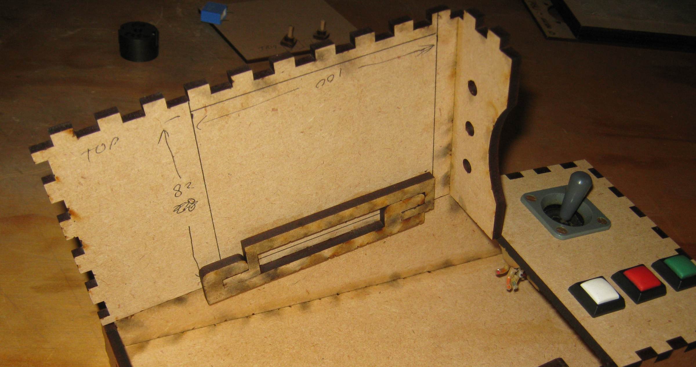
Module locking, with PCB outline in pencil and dummy CRT front
What is less obvious from the photograph of the module locking is that the user interface panel (joystick, push buttons) stops the CRT module from withdrawing, hence locking it in place.
Mechanical design packages
Inkscape, with the ‘The Laser Cut Box’ extension was used to design the initial top and bottom enclosures. The only real aesthetic binding the two designs is the frequency of the interlocking castellations. The resulting design from inkscape was simply cut and pasted into Autosketch, where the remaining edits were made to form the two enclosures.
The units were fabricated from MDF using a 70W laser cutter. This unit allowed extremely fast turnaround which allowed alternate design ideas to be tried out quite quickly.
Conclusion
As was hoped, masses-of-stuff was learnt from this project since (with the exception of the embedded processor) everything was outside my run-of-the-mill experiences.
Clearly, there are plenty of other games, and applications possible for this stand-alone, general purpose, vector based drawing machine. I really must get around to attaching an I2C clock module to the CPU board and adding the analogue clock option. There are obviously many other games possible, but one step at a time.
Apart from the embarrassing cock-up of the wrong mini-B USB footprint, and my first attempt at (unsuccessfully) using a current-DAC in voltage mode, I am not sure what I would do differently next time. The project certainly met all of its initial targets in terms of education, and as is always the case, there were some surprises along the way.
Mark Atherton, New Zealand, 19 July 2020, markaren1@xtra.co.nz
This article is published under the Creative Commons Attribution License (cc-by). Re-distribution and re-use of this work is on the condition that the creator (Mark Atherton, New Zealand) is appropriately credited.