 zpekic
Converting incompatible video standards especially in retrocomputing field is a well-known problem, for which a whole cottage industry has been created (e.g. GONBES and similar).
To recap:
| TIM-011 | VGA (basic mode) | |
| Color info | Digital, 4 level, 2 signals | Analog, 3 signals, theoretically 2^24 colors with 3 8-bit DACs |
| Pixel clock | 12MHz | 25.125MHz (25Mhz is used for design simplicity) |
| Horizonal sync | 15.625kHz | 31.25kHz |
| Vertical sync | 50Hz | 60Hz |
As can be seen from the above, any simple or "passive" connectivity between the two won't work. The apparent solution is to:
- Capture input signal (synchronized to TIM-011 timing)
- Store video data in memory (buffer)
- Generate output signal from memory (as VGA)
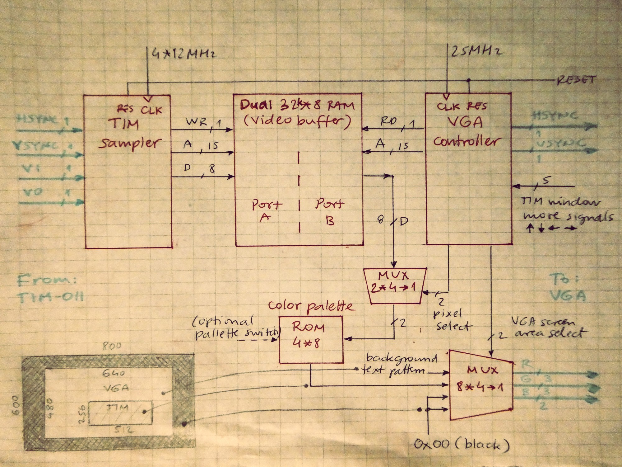
In the code, the key components behind this are:
As expected, the component input matches TIM-011 signals, and the output the simple RAM interface to be able to write to 32kB RAM:
entity tim_sampler is
    Port ( reset : in  STD_LOGIC;
           clk : in  STD_LOGIC;
           hsync : in  STD_LOGIC;
           vsync : in  STD_LOGIC;
           v2 : in  STD_LOGIC;
           v1 : in  STD_LOGIC;
           a : out  STD_LOGIC_VECTOR (14 downto 0);
           d : out  STD_LOGIC_VECTOR (7 downto 0);
           limit: in STD_LOGIC_VECTOR (5 downto 0);
           we_in: in STD_LOGIC;
           we_out : out  STD_LOGIC);
end tim_sampler;
The clk is multiple of 12MHz to match TIM-011 signals. This can be generated by higher level component using PLL on FPGA, but I simply added a 48MHz external crystal as it is fun to play with them if the board allows.
Critical input to observe is the hsync signal - we know that when it goes from high to low, TIM-011 will start a scan line of 512 dots, each 83.3ns duration (1 / 12MHz). The idea then is to wait for this transition, and when happens, sample the v1 and v2 video inputs with overscan frequency (4 times multiple in this case).
There is some arithmetic behind this:
1 byte to write to RAM == 4 pixels == 16 bits
Therefore, after 16 bits "shifted in" from v1 and v2, the byte has to be written to memory.
In order to make sampling even more effective, it is done both on rising and falling edge of the 48MHz clock, and because FPGAs allow 1 clock per register, effectively there are 3 16 bit registers per video signal one for rising, one for falling and one that combines them:
signal s2, s1, s2r, s2f, s1r, s1f: std_logic_vector(15 downto 0);
signal h: std_logic_vector(10 downto 0);
signal v: std_logic_vector(8 downto 0);
signal sample: std_logic_vector(7 downto 0);
Other signals:
h - goes from 0 to 511, therefore 10 bits are needed because counting can go on until next hsync signal but should not generate RAM write (not sure why I added 1 extra bit?)
v - goes from 0 to 255, but one extra bit as vsync takes time too and count runs
sample - byte to be written to RAM
s2 and s1 are combination of signals captured at clk rising and falling. To experiment, the circuit allows combining them with "or" or "and":
generate_s: for i in 15 downto 0 generate
begin
    s2(i) <= ((not limit(5)) and s2r(i) and s2f(i)) or (limit(5) and (s2r(i) or s2f(i))); --(s2r(i) or s2f(i));
    s1(i) <= ((not limit(5)) and s1r(i) and s1f(i)) or (limit(5) and (s1r(i) or s1f(i))); --(s1r(i) or s1f(i));
end generate;
Note that the for loop is BUILD time, not RUN time (so nothing "runs the loop" on FPGA, but the VDHL synthesis generates circuitry as if s2(15) <= ... s1(15) <= ... lines of code would have been written 32 times.
With this we now have 16 bit s2 signal (captures v2 video) and 16 bit v1 signal. But the RAM byte has 1 bit per each, so we need to convert 16 => 4, generating the "sample".
How is "sample" generated? One has to decide if the video signal was present or not. This is where the "voter" circuit comes in. Based on how many of 4 sample pixels were detected as "1" and the experimentation setting, it returns the vote of "1" or "0" by default:
    with value select vote <=
        '1' when "1111",
        limit(4) when "1110",
        limit(3) when "0111",
        limit(2) when "1100",
        limit(1) when "0110",
        limit(0) when "0011",
        '0' when others;
As there are 8 bits in the "sample" obviously, 8 "voters" are needed, hooked up to right s1, s2 inputs and sample byte bits:
Finally, sample byte needs to be written to RAM:
            case h(3 downto 0) is
                when X"F" =>
                    d <= sample;
                    a <= v(7 downto 0) & h(10 downto 4);
                when X"1" =>
                    we_out <= we_in and (not v(8));
                when X"E" =>
                    we_out <= '0';
                when others =>
                    null;
            end case;
As the h counter runs, we inspect the least significant nibble:
0 ... no operation
1 ... D - write last sample with captured address
E - disable write signal to prevent any overlap glitch
F - capture sample and address to be written in subsequent 16 clock cycle. Note the address schema aligned with TIM-011 video generation hardware described here:
- 128 bytes are used for line 0, then 128 for line 1 etc., meaning that the upper 8 bits of address are "rows" and lower 7 bits are "columns".
As can be seen, the memory write bandwith is pretty low: 48MHz/16 = 12MHz/4 = 3MHz.
Vertical signal processing:
This is simple, at each hsync signal, the vertical count needs to be incremented, and when vsync goes high (one full frame has been captured), it needs to be reset to 0:
on_hsync: process(hsync, reset, vsync)
begin
    if ((vsync or reset) = '1') then
        v <= "000000000";
    else
        if (rising_edge(hsync)) then
            v <= std_logic_vector(unsigned(v) + 1);
        end if;
    end if;
end process;
Note that hsync triggers even after 256 lines, incrementing v. This would cause "good" video info to be overwritten with "no data" as the v counter wraps around. That's why the write logic only work when v(8) == '0', meaning for first 256 lines only. I spent about a week of my life and near nervous breakdown before I found this bug.
VIDEO BUFFER RAM - ram32k8_dualport.vhd
To store 512*256 4 color pixels, 32kBytes of RAM are needed (15 bit address, 8 bit data width). This RAM needs to be:
- written by TIM signal sampler
- read by VGA controller
Given that there are 2 possible approaches:
Single port RAM
The 2 components would need to share a common address, data, control bus in a time multiplexed fashion. Given that we VGA controller needs to generate video signal continuously, it would need the priority to access RAM any time not "drawing off screen" (meaning either hync or vsync are active to simplify a bit). The sampling runs in parallel and continuously, which means that some samples would need to be dropped. This is not really a problem as even moderate speed animations are rather static, perhaps few frames per second, so in the worst case on VGA user would see frame 1 then 4 but not 2 and 3. When image is static (text, graphics), dropped samples would not be perceived at all, simply the circuit would catch up after few 1/50s frame cycles.
Dual port RAM
This is "partial" dual port as 1 port always writes (TIM sampler) and 1 always reads (VGA controller). The FPGA I used has the capacity and "IP" component that does this nicely so I used it:
LIBRARY ieee;
USE ieee.std_logic_1164.ALL;
-- synthesis translate_off
LIBRARY XilinxCoreLib;
-- synthesis translate_on
ENTITY ram32k8_dualport IS
  PORT (
    clka : IN STD_LOGIC;
    ena : IN STD_LOGIC;
    wea : IN STD_LOGIC_VECTOR(0 DOWNTO 0);
    addra : IN STD_LOGIC_VECTOR(14 DOWNTO 0);
    dina : IN STD_LOGIC_VECTOR(7 DOWNTO 0);
    clkb : IN STD_LOGIC;
    addrb : IN STD_LOGIC_VECTOR(14 DOWNTO 0);
    doutb : OUT STD_LOGIC_VECTOR(7 DOWNTO 0)
  );
END ram32k8_dualport;
VGA SIGNAL GENERATION - vga_controller.vhd
There are many different and available VHDL / Verilog implementations of VGA controllers, from the simplest to most complex ones. For the job at hand, I decided to write another one because of some extra requirements:
- custom pixel layout in memory
- conversion of 4 "colors" to VGA colors
- positioning of 512*256 TIM "window" on 640*480 VGA screen
- differentiating when video display info needs to come from "TIM window" (from buffer RAM), or not (area outside of TIM window)
Therefore the component definition is a bit different than expected:
entity vga_controller is
    Port ( reset : in  STD_LOGIC;
           clk : in  STD_LOGIC;
           offsetclk: in STD_LOGIC;
           offsetcmd: in STD_LOGIC_VECTOR(3 downto 0);
           hsync : buffer  STD_LOGIC;
           vsync : out  STD_LOGIC;
           h_valid: buffer STD_LOGIC;
           v_valid: buffer STD_LOGIC;
           h : buffer STD_LOGIC_VECTOR(9 downto 0);
           v : buffer STD_LOGIC_VECTOR(9 downto 0);
           x_valid: out STD_LOGIC;
           y_valid: buffer STD_LOGIC;
           x : out  STD_LOGIC_VECTOR (8 downto 0);
           y : out  STD_LOGIC_VECTOR (7 downto 0));
end vga_controller;
offsetclk, offsetcmd:
allow the TIM window to be moved up/down/left/right within VGA screen. These are hooked up to Mercury baseboard push-buttons and their effect can be seen on the video.
hsync, vsync:
standard VGA sync signals, only 1 mode is supported timing-wise
h_valid, v_valid, h, v:
VGA pixel coordinates and if in valid horizonal and vertical range
x_valid, y_valid, x, y:
TIM pixel coordinates and if in valid horizontal and vertical range
Internally, the registers are updated in two processes, driven by 2 clocks:
1. 25MHz dotclk (lines 116 - 142)
Two key registers updated are:
h_cnt - free incrementing counter with each dotclk (position across the line, but note that includes invisible part of the line too)
h_index - pointer to one entry of the following table:
signal h_signal: signal_lookup := (
    "000000" & std_logic_vector(to_unsigned(95, 10)), -- hsync
    "010000" & std_logic_vector(to_unsigned(47, 10)), -- no signal
    "011010" & std_logic_vector(to_unsigned(63, 10)), -- h_active
    "011100" & std_logic_vector(to_unsigned(511, 10)), -- h_active, x_valid
    "011011" & std_logic_vector(to_unsigned(63, 10)), -- h_active
    "110000" & std_logic_vector(to_unsigned(15, 10)), -- reset at the end
    "110000" & std_logic_vector(to_unsigned(15, 10)), --
    "110000" & std_logic_vector(to_unsigned(15, 10))  --
);
The process starts with h_cnt 0 and h_index 0, and the highlighted "000000" is connected to hsync which is low active. This state goes on until h_cnt hits value of 95, after which h_index increments to 1, and h_cnt is reset to 0, to count towards 47 etc. This is very similar how old washing machine programators worked, pipes and motor actuators are top 6 bits, and lower 10 are time interval measured before kicking into different wet / dry / tumble cycle.
Note the 63 - 511 - 63 pattern - this is how the TIM window is positioned horizontally on the screen, centered with 64 pixels on each side. Obviously, if we could change this to 62 - 511 - 64 that would mean TIM window moved 1 pixel left. This change is the job of the "offset register" component:
h_off: offsetreg Port map (
                reset => reset,
                initval => std_logic_vector(to_unsigned(63, 10)),
                mode => offsetcmd(1 downto 0),
                clk => offclk,
                sel => h_sel,
                outval => h_offset
            );
When looking at the implementation of offsetreg.vhd it is obvious what the "mode" does - push on one button or other increments / decrements the opposite offsets, and pressing both puts them back to initial state (centers the window):
            case mode is
                when "01" =>
                    p_reg <= std_logic_vector(unsigned(p_reg) + 1);
                    n_reg <= std_logic_vector(unsigned(n_reg) - 1);
                when "10" =>
                    p_reg <= std_logic_vector(unsigned(p_reg) - 1);
                    n_reg <= std_logic_vector(unsigned(n_reg) + 1);
                when "11" =>
                    p_reg <= initval;
                    n_reg <= initval;
                when others =>
                    null;
            end case;
There are two registers in the component, p_reg and n_reg which count in opposite direction, as left / right and top / bottom margins are opposite. At the right h_index and v_index, the hard-coded values of margins ("h_current") are replaced with value coming from offset reg (h_offset):
h_limit <= h_offset when (h_reg = '1') else h_current(9 downto 0);
2. 31.25kHz vertical (vsync) clock
At end of each horizontal line (per hsync), the vertical counter needs to be updated. The logic and the process is same like for horizontal signal, but the timing constants obviously different:
signal v_signal: signal_lookup := (
    "000000" & std_logic_vector(to_unsigned(1, 10)), -- vsync
    "010000" & std_logic_vector(to_unsigned(32, 10)), -- no signal
    "011010" & std_logic_vector(to_unsigned(111, 10)), -- v_active
    "011100" & std_logic_vector(to_unsigned(255, 10)), -- v_active, y_valid
    "011011" & std_logic_vector(to_unsigned(111, 10)), -- v_active
    "110000" & std_logic_vector(to_unsigned(9, 10)), -- reset at the end
    "110000" & std_logic_vector(to_unsigned(9, 10)), --
    "110000" & std_logic_vector(to_unsigned(9, 10))  --
);
It is obvious that top and bottom margin are now 112 rows (lines) and are being replaced by values coming from vertial offset register. Note highlighted 10 and 11 in the table. 1 on bit position 11 flips the MUX to take the value from offset reg, and 1 on bit 10 controls if the offset reg will serve out "p_reg" or "n_reg".
CONNECTING it all together - sys_tim011_mercury.vhd
Component on the higher level of hierarchy connects the sampler, the RAM, and the VGA controller.
Maybe it is easiest to follow the signals from R, G, B pins backward.
The Mercury base-board has a simple resistor ladder DAC with total resolution of 8 bits, 3 red, 3 green, 2 blue. These bits come from a generate "vga_color" byte
-- now convert to VGA 8-bit color
RED <= vga_color(7 downto 5);
GRN <= vga_color(4 downto 2);
BLU <= vga_color(1 downto 0);
Now remember that an any moment the "electron beam" (or its virtual equivalent on LCD) can only be:
- outside of screen - use color black
- in TIM window - use 1 out of 4 TIM colors as an index into a 4 entry color byte palette
- outside TIM window, but in VGA area - for fun, just generate a text screen background
Like everything else, the above is just a MUX:
-- color index also takes into account selected palette and if in TIM window
color_sel <= vga_window & tim_window;
with color_sel select vga_color <=
    text_color when "10",                                                        -- text outside tim window
    tim_color(to_integer(unsigned(switch(0) & pair))) when "11",    -- tim pixel
    color_black when others;
What is color_sel? Simply a combination of signals from VGA controller indicating in which display window is the "beam":
tim_window <= x_valid and y_valid;
vga_window <= v_valid and h_valid;
The "pair" is actual 2 video bits V1 and V0 stored in the video buffer RAM. These are selected by looking at the lowest 2 bits of the x (horizontal) value the VGA controller outputs:
-- pixels are stored 11003322
-- see https://github.com/zpekic/Sys_TIM-011/blob/master/Img2Tim/Img2Tim/Program.cs
with vga_x(1 downto 0) select pair <=
    vram_douta(5 downto 4) when "00",
    vram_douta(7 downto 6) when "01",
    vram_douta(1 downto 0) when "10",
    vram_douta(3 downto 2) when others;
It is interesting to note how the pixels are stored in a byte - not in an expected way but shuffled around in the nibbles. As the lower 2 bits of x go from 00 to 11, selection of the "pair" needs to follow the storage pattern.
Obviously these bits have to come from vram_douta data port "B" (naming bug!) which is connected to the VGA controller. But where is the RAM address coming from on VGA side?
vga_a <= vga_y & vga_x(8 downto 2);
As expected, one "line" (vga_x) is stored in 128 bytes and then there are 256 such lines (blocks of RAM) down the rows (vga_y).
The other RAM port is connected to the sampler, and is write only, when allowed (vram_wea signal generated by sampler):
mem: ram32k8_dualport PORT MAP(
-- sampler only writes
    clka => byteclk,
    ena => '1',
    wea => vram_wea,
    addra => sampler_a,
    dina => vram_dina,
-- vga only reads
    clkb => CLK,
    addrb => vga_a,
    doutb => vram_douta
  );
(small bug: vram_douta should be renamed to vram_doutb)
The actual "tim_color" is a lookup into a small 8 bytes entry ROM. The lower 2 bits are selected by V1 and V0 from buffer RAM (== TIM video signal intensity), and just for fun the upper address bit is connected to switch for instant selection of grayscale or color display:
constant color_black:    std_logic_vector(7 downto 0):= "00000000";
constant color_blue:    std_logic_vector(7 downto 0):= "00000011";
constant color_green:    std_logic_vector(7 downto 0):= "00011100";
constant color_cyan:    std_logic_vector(7 downto 0):= "00011111";
constant color_white:    std_logic_vector(7 downto 0):= "11111111";
constant color_red:    std_logic_vector(7 downto 0):= "11100000";
constant color_yellow:    std_logic_vector(7 downto 0):= "11111100";
constant color_ltgray:    std_logic_vector(7 downto 0):= "01101101";
constant color_dkgray:    std_logic_vector(7 downto 0):= "10010010";

type color_lookup is array (0 to 7) of std_logic_vector(7 downto 0);

signal tim_color: color_lookup := (
    -- grayscale palette
    color_black,    -- tim pixel 00
    color_dkgray,    -- tim pixel 01
    color_ltgray,    -- tim pixel 10
    color_white,    -- tim pixel 11
    -- colorful palette
    color_black,    -- tim pixel 00
    color_yellow,    -- tim pixel 01
    color_cyan,    -- tim pixel 10
    color_green    -- tim pixel 11
    );
Discussions
Become a Hackaday.io Member
Create an account to leave a comment. Already have an account? Log In.