0%
0%
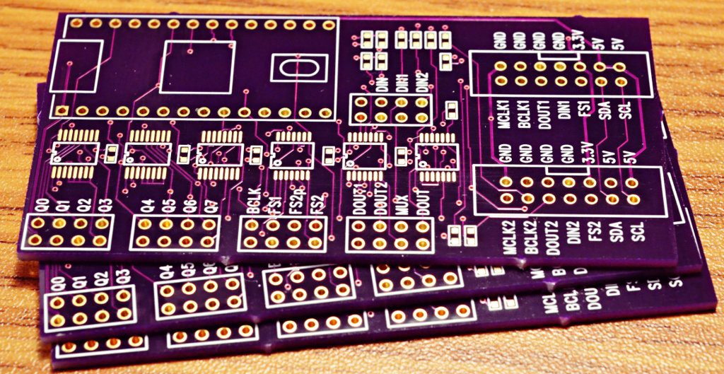
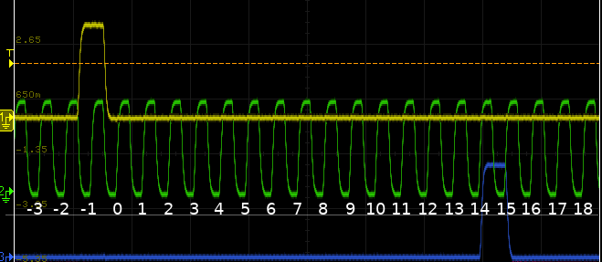
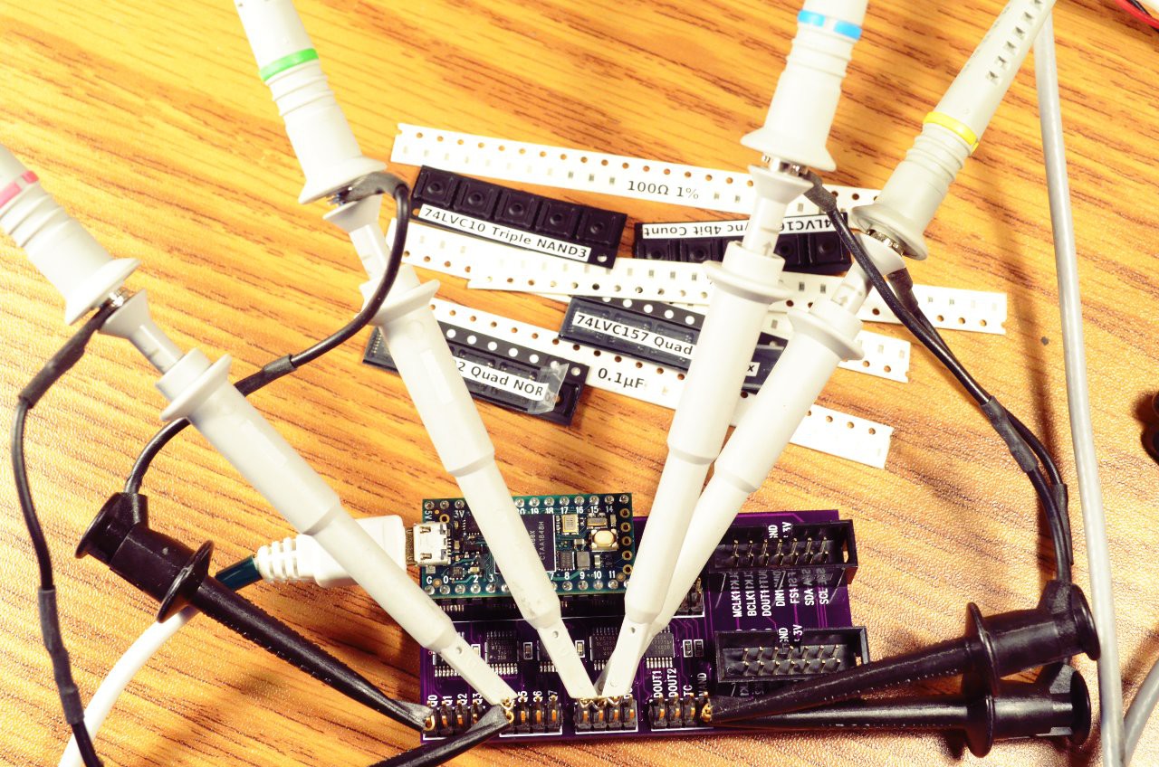
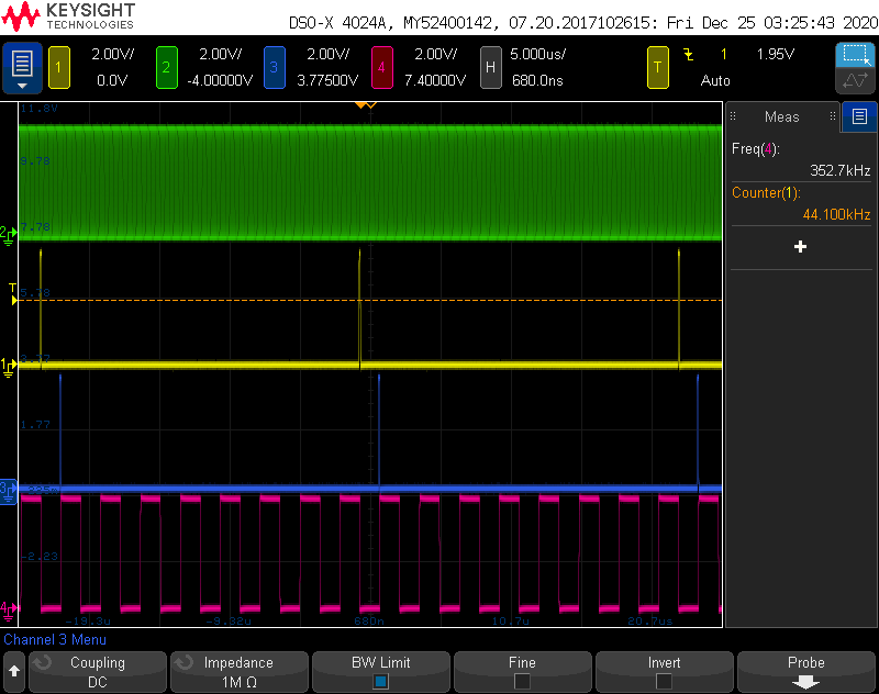
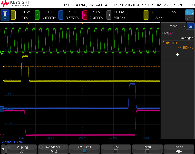
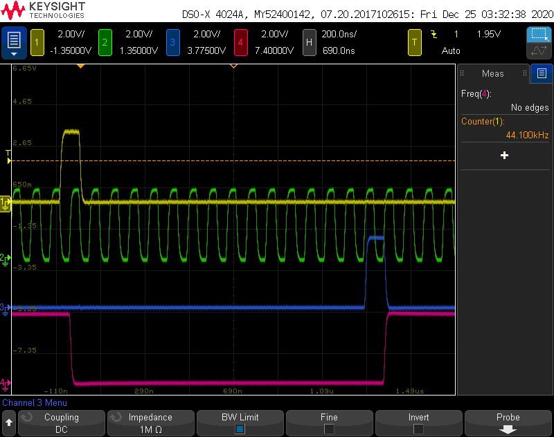
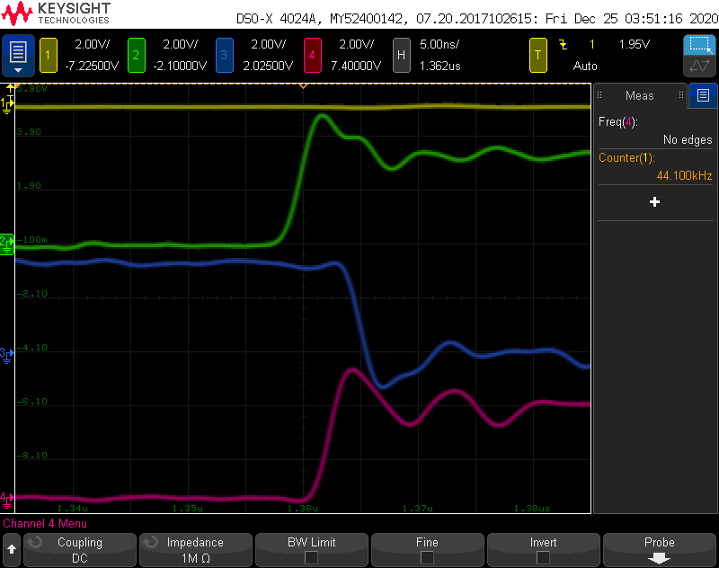
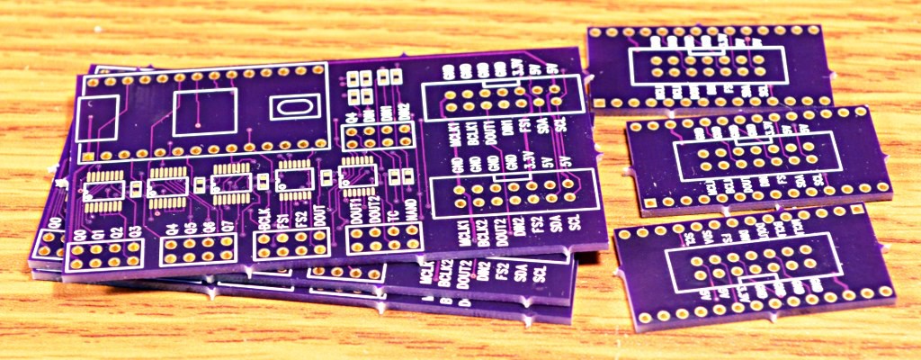
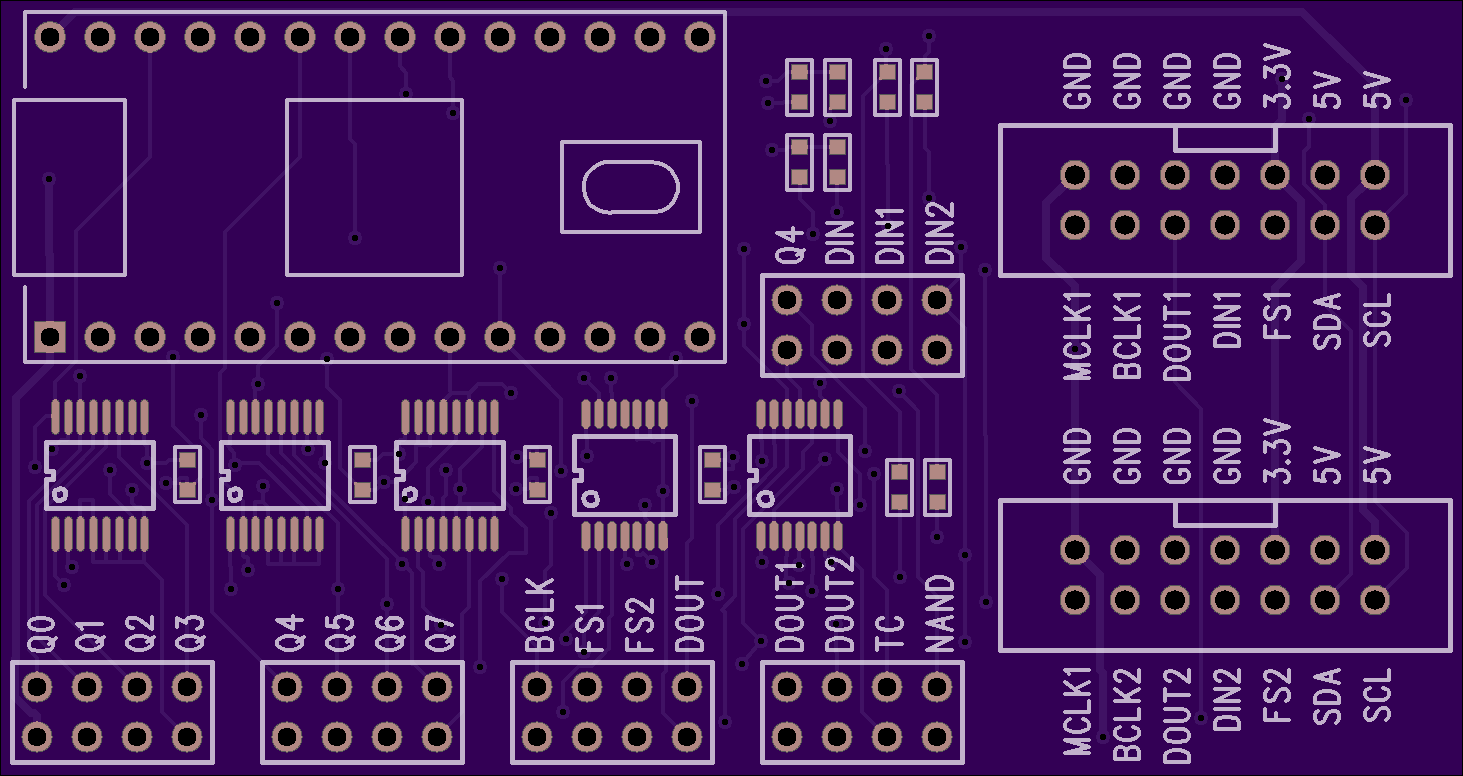
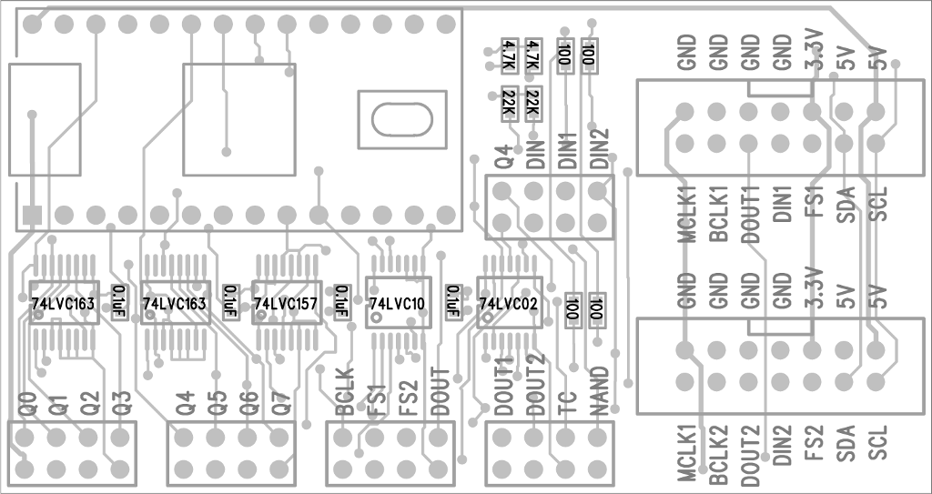
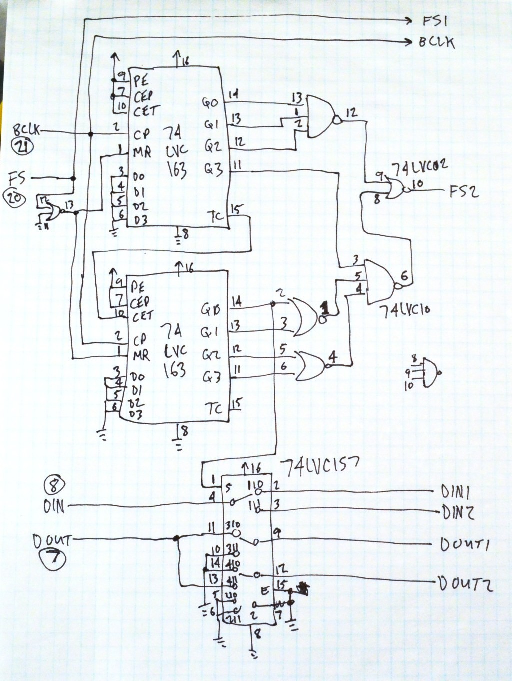
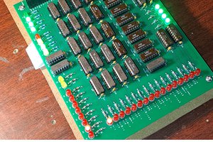
Dual Interleaved CS42448 Chip
16 Audio In & 16 Audio Out using only 5 pins
 Paul Stoffregen
Become a Hackaday.io member
Already have an account? Log in.
Just one more thing
To make the experience fit your profile, pick a username and tell us what interests you.
Pick an awesome username
hackaday.io/
Your profile's URL: hackaday.io/username. Max 25 alphanumeric characters.
Pick a few interests
Projects that share your interests
People that share your interests

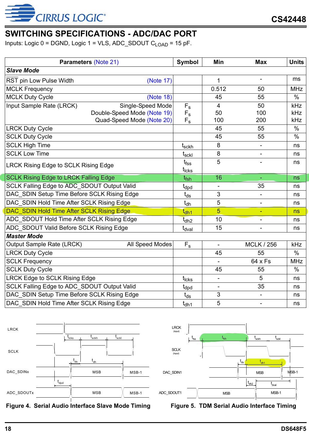
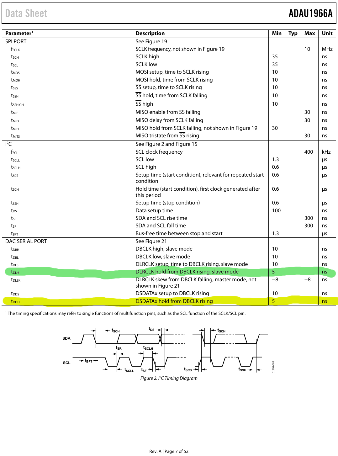
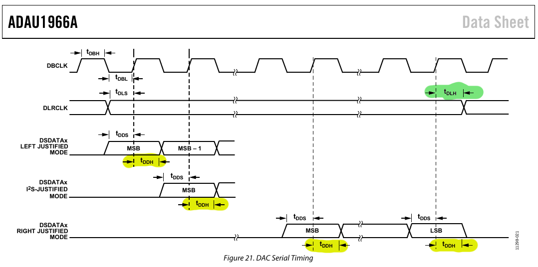 Analog Devices really shows how to compose a good timing diagram. The dotted lines from the clock edges to only the meaningful timing specs really helps communicate which things matter. Nice!
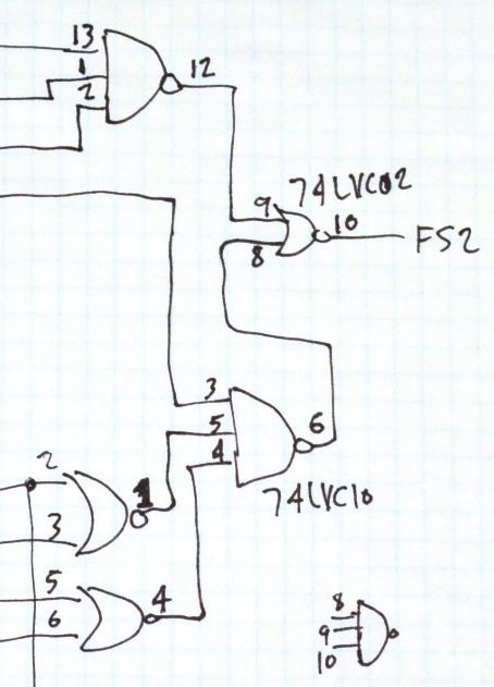

 Nicolas REIMEN
 Jon Thomasson
 matseng
 Michael Kafarowski
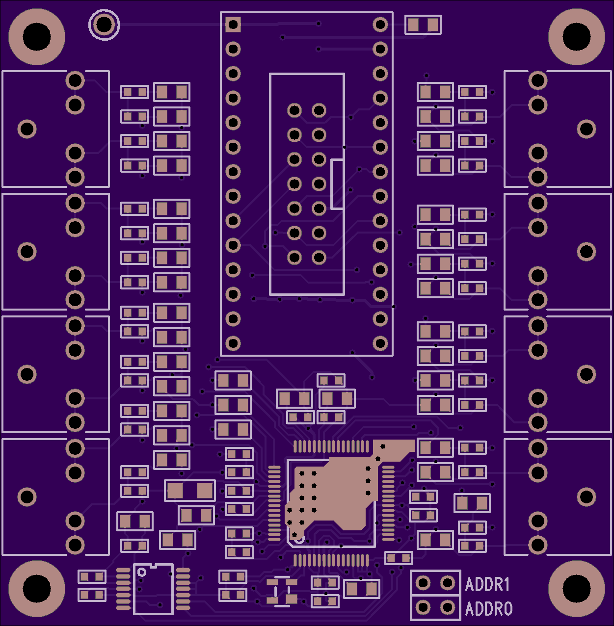
Very excited to follow this build Paul! Ive tried and failed at designing PCBs around the
CS42448 and CS5368 so i will be following closely.