 txyz.info
PCB Delayering
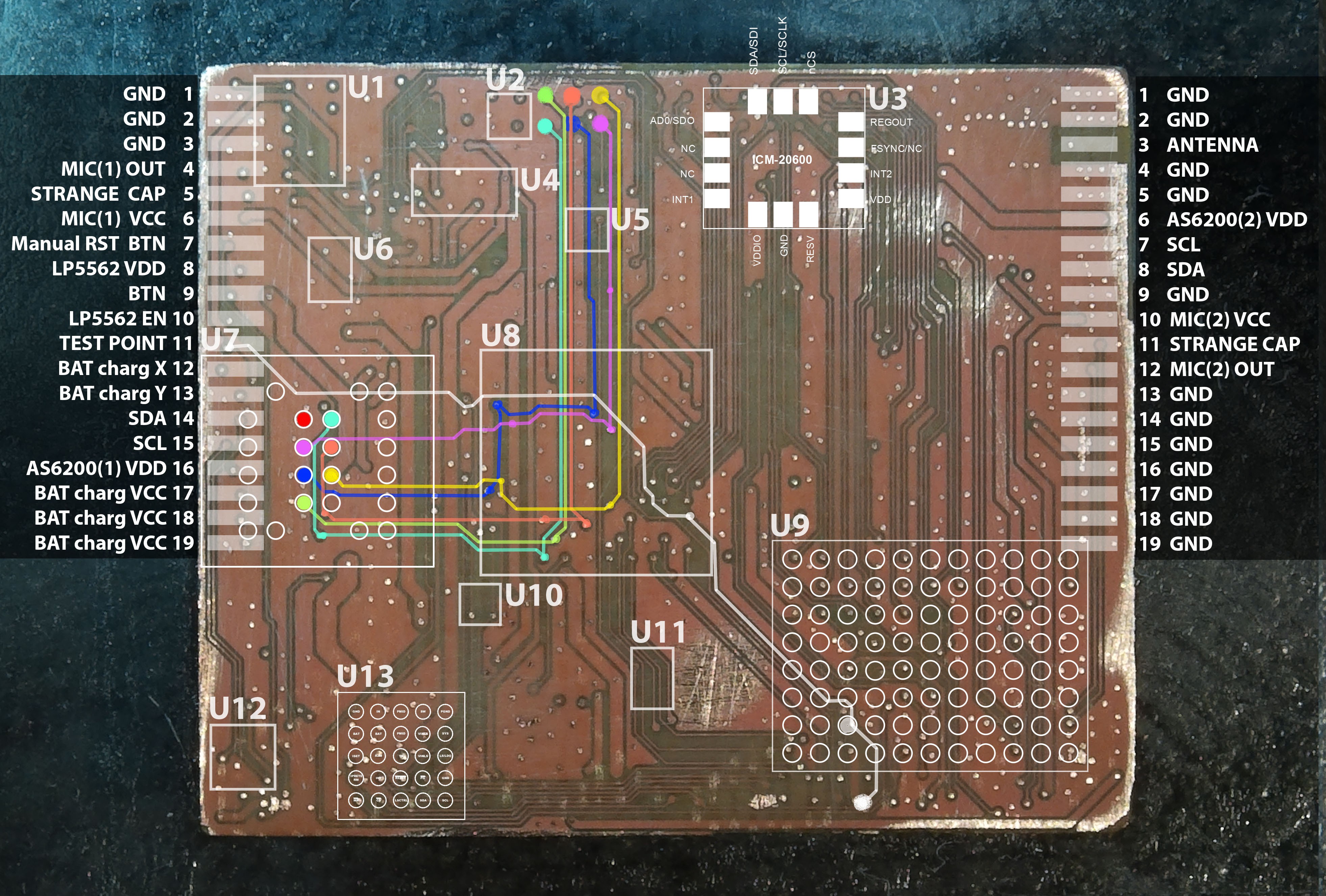
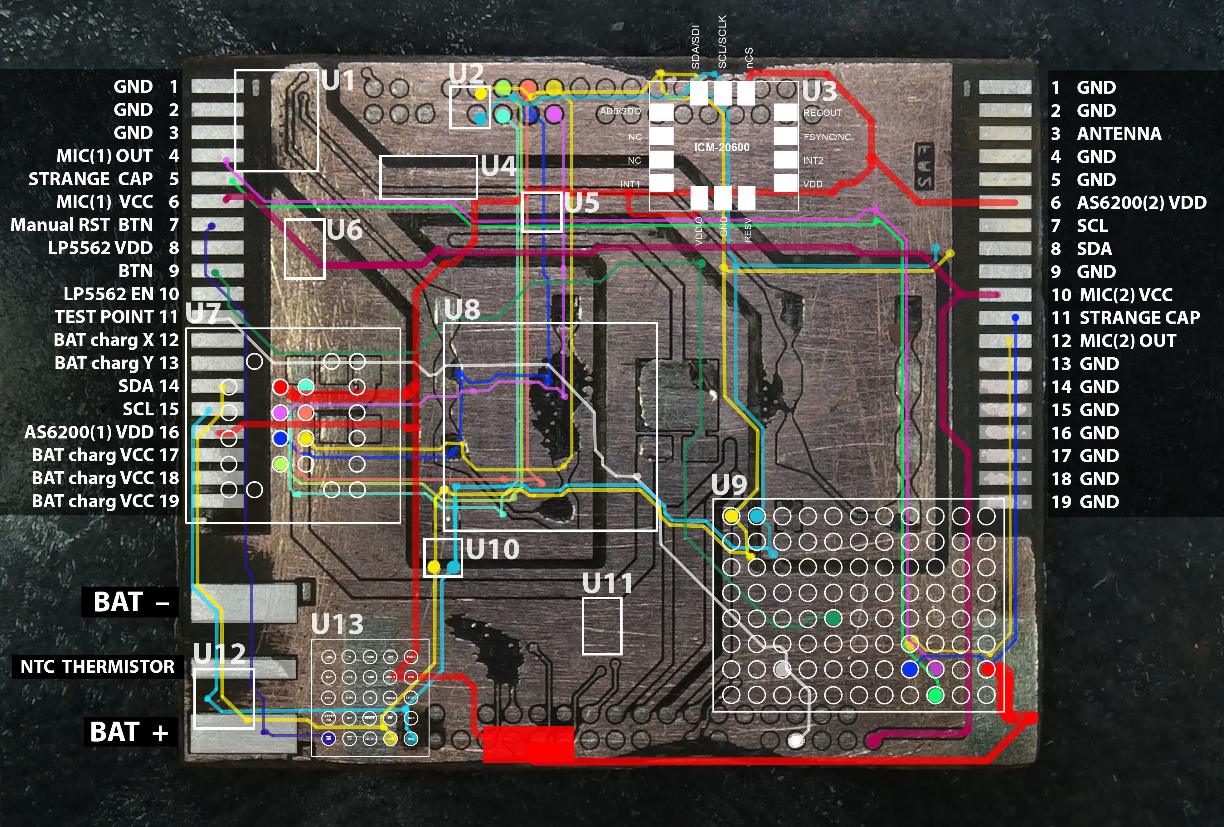
I was hoping to find marking codes on the BGA chips while decapping the main chip(SiP), but found nothing. So I decided to look inside the PCB layers and hopefully get some clues.
The delayering process was straightforward, using Sandpaper, Double-sided tape, and a piece of glass on which I mounted an extremely thin PCB.
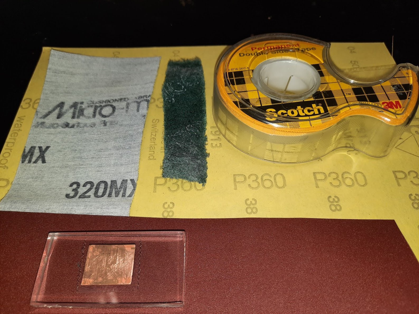
PCB delayering was a success, I uncovered 3 part numbers:
- U3 - IMU ICM-20600
- U7 - flash memory MT25QU256ABA
- U13 - battery charger BQ25125
PCB has 5 copper layers, with the ground plane in the middle.
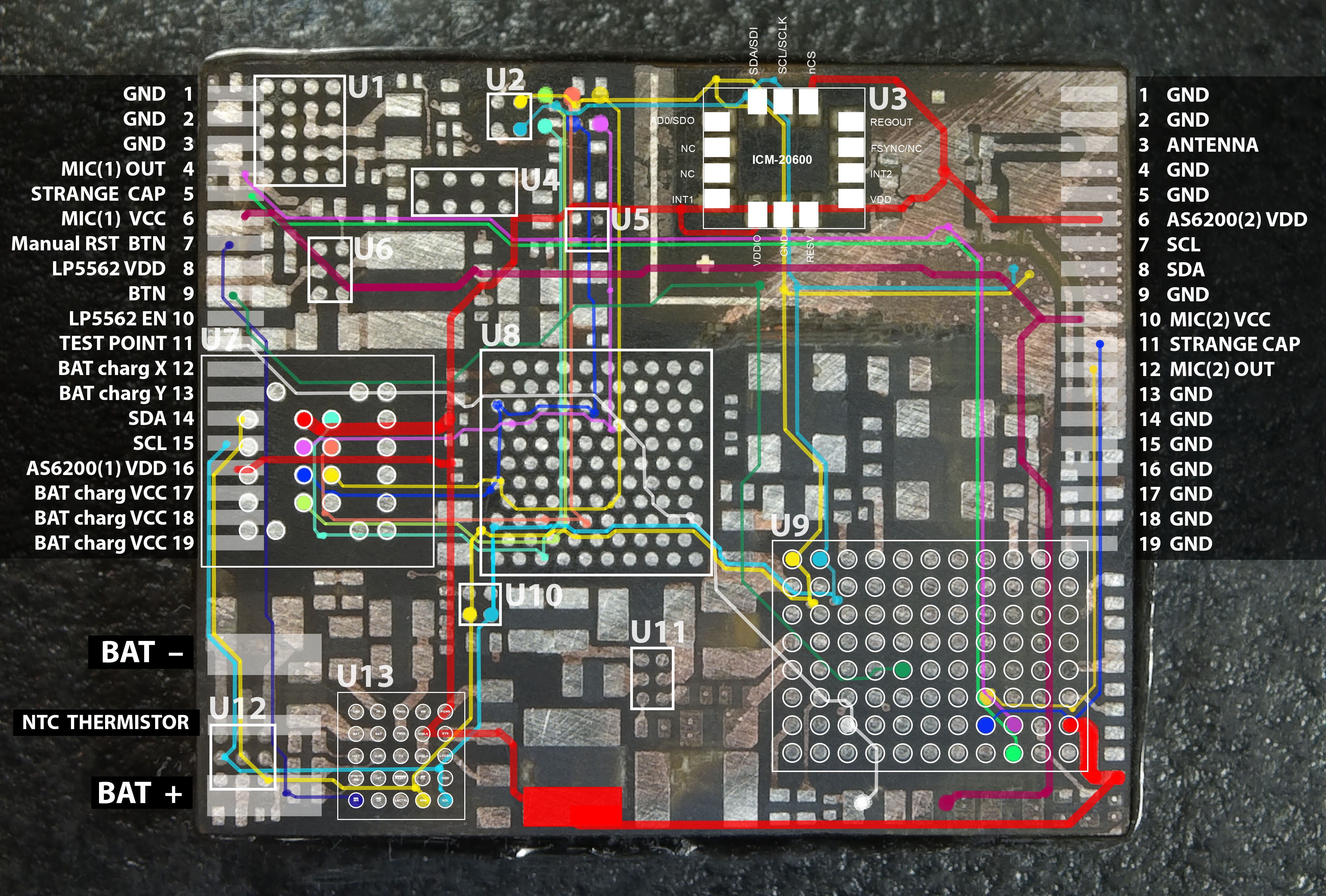
Mics and strange Caps
PCB reverse-engineering begins with a weird discovery: a capacitor from flex PCB that is connected to the pin on BLE SOC U9, unusually far away from U9.
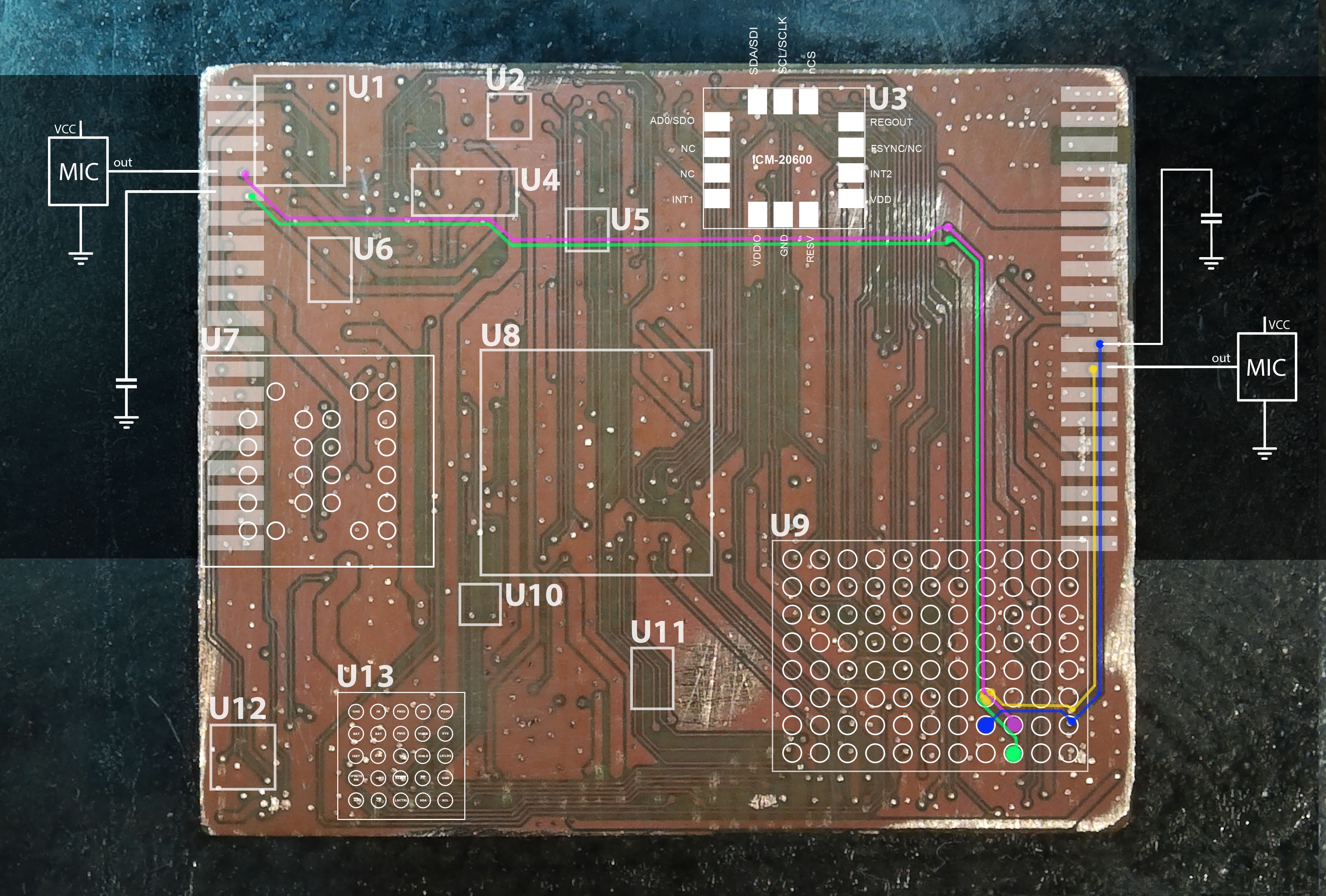
Button
Button connected to the main PCB with 2 traces from flex PCB, another strange design choice.
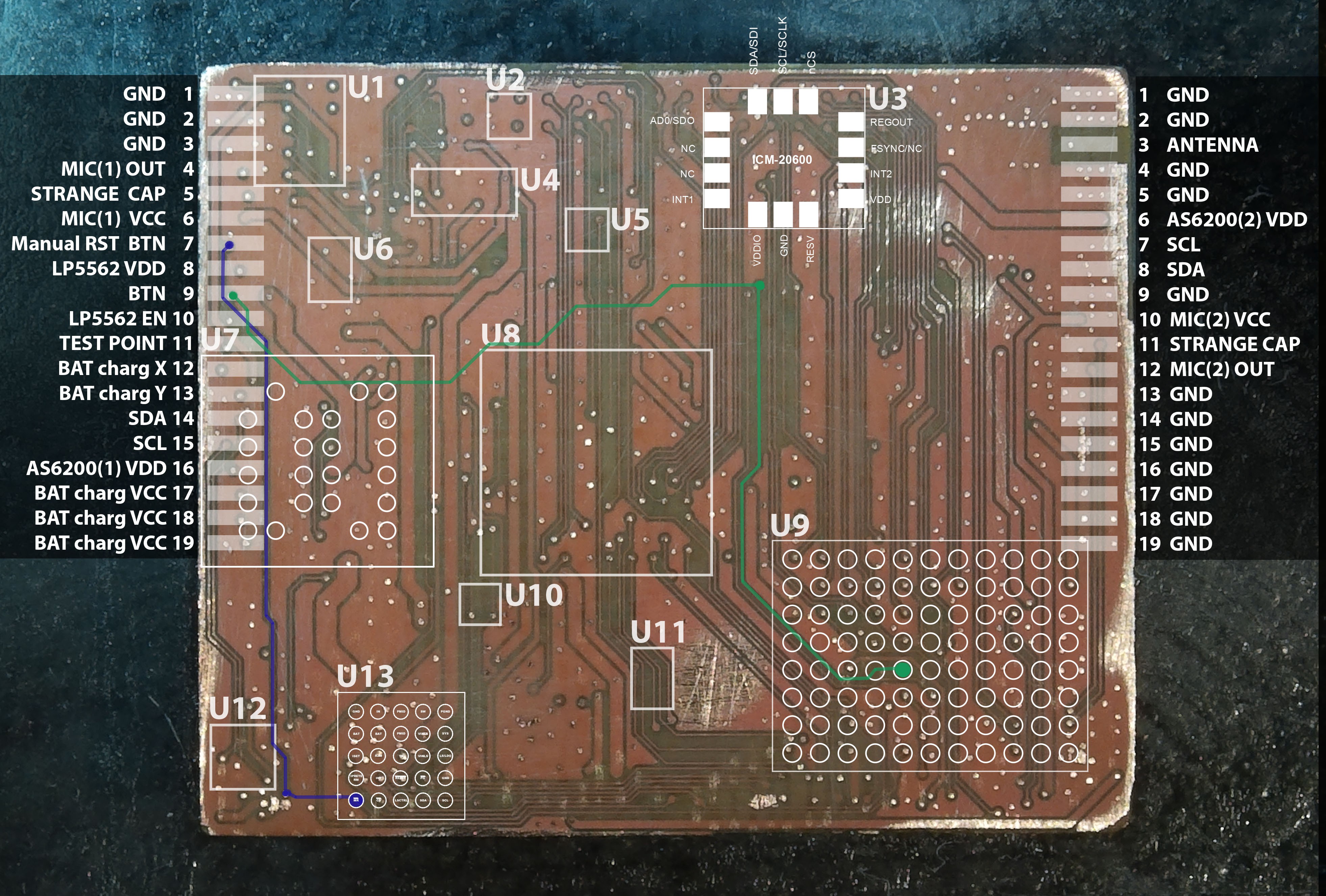
i2c
The chip design continues to get weirder: i2c lines are not connected to the pads on the right side! This means the second i2c temperature sensor located on flex PCB is useless.
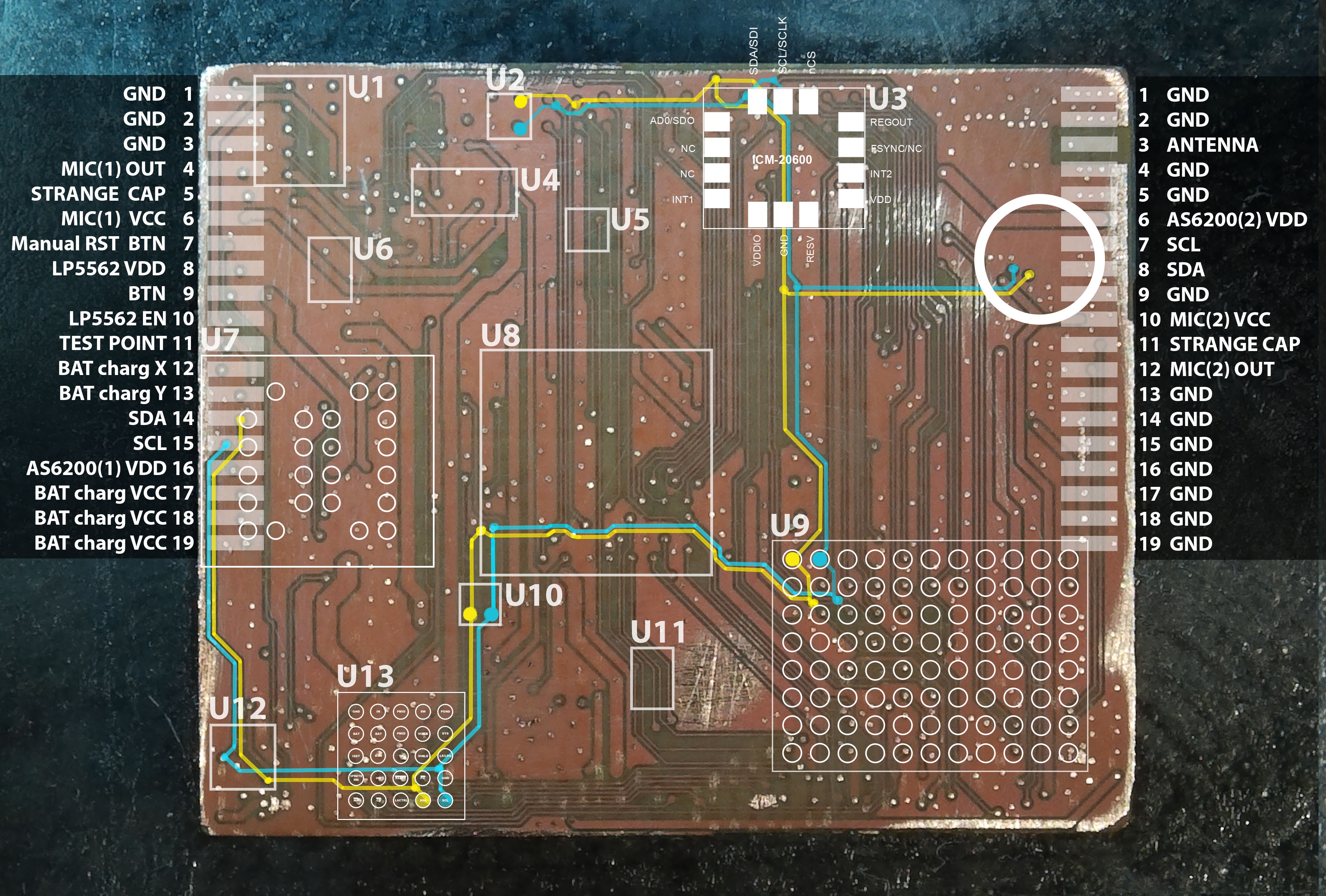
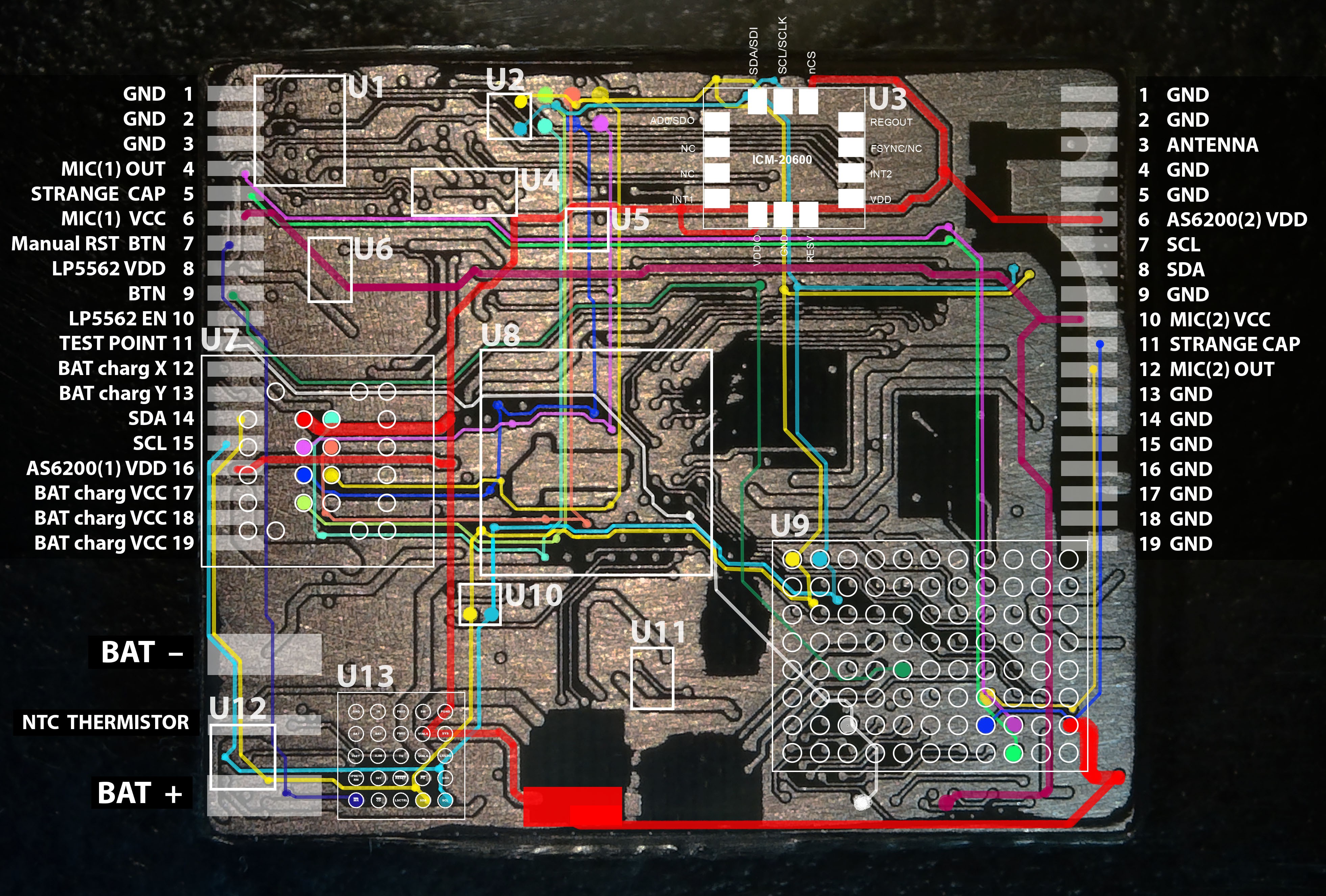
Flash memory
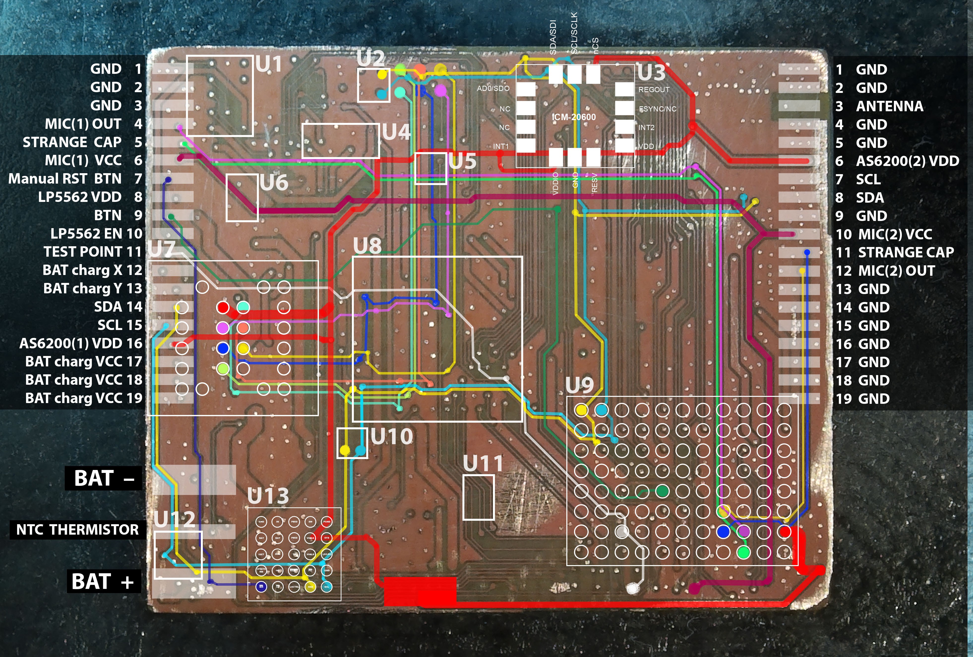
All together with power lines
Future plans
"2008-002100-21 Project-D" has a lot of test points where I want to connect JTAGulator and GoodFET, in order to do this I need to order another Halo.
Discussions
Become a Hackaday.io Member
Create an account to leave a comment. Already have an account? Log In.