hesam.moshiri
Specifications
Input Voltage (max): 35V [30V, max-tested]
Output Voltage (min): 1.28V
Output Voltage (max-tested): 27.35V [28.9Vin, no load, 25C]
Output Current: 1.1mA to 4A(max continous)
Output Noise (no load): 6-7mVpp
Output Noise (1A load): 6-7mVpp
Output Noise (2A load): 8-10mVpp
Note: This is the first prototype, as I have mentioned in the video, in the last revision of the PCB board (which is available for you), the distance between electrolytic capacitors and the power resistors has been increased, however, if you still have concerns about this, you can use 470uF-50V capacitors instead of 1000uf-50V capacitors which are smaller in diameter.
A: Circuit Analysis
Figure 1 shows the schematic diagram of the device. The design consists of two main parts: the main regulator circuit and the current limiting circuit.
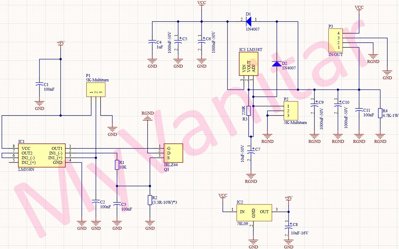
Figure 1, Schematic diagram of the adjustable power supply
P3 is the KF128-4Pin block terminal to connect the input and output wires to the circuit. C4, C5, and C6 are used to reduce input noise. D1 and D2 are protective diodes. Schottky diodes can be used instead of D1 and D2 as well.
IC3 is the LM338 5A positive linear regulator [1]. R3 provides an output feedback path to the regulator and P2 is a 5K multiturn potentiometer that is used to adjust the output voltage. C7 capacitor has been used to reduce noise. C9, C10, and C11 have been used to reduce output noise, however, they are connected to another ground reference that is the Drain pin of Q1.
Q1 is the IRLZ44 N-Channel Mosfet [2] that limits the current with the help of IC1. The theory behind how the combination IC1 and Q1 does the current limiting is a bit complex and it will be explained in a video in the future. IC1 is the LM358 famous operational amplifier [3]. R2 is the load resistor that consists of three 3.3R-10W resistors in parallel, which is equal to a 30W-1.1R resistor.
C3 and R1 build an RC filter that reduces the noises coming from the load resistor. C1 and C2 are also used to reduce noise. IC2 is a 78L09 regulator [4] that is used to provide a stable supply rail for the IC1. C8 has been used to reduce the output noise of the IC2. P1 is a 5K multiturn potentiometer that is used the set the current limit. Finally, R4 is a basic load resistor that draws a few milliamperes of current to stabilize the output of the power supply under no load.
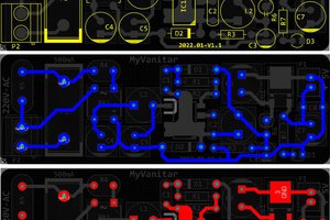
B. PCB Layout
Figure 2 shows the last revision of the PCB layout. It’s a two layers PCB board and all component packages are through-hole. Pretty easy to solder for most users. The thickness of high current carrying tracks is 4.5mm. You should mount three 3.3R-10W resistors on top of each other to build R2, so R2 is a parallel resistor of three 3.3R-10W resistors, that is equal to a 1.1R-30W resistor.
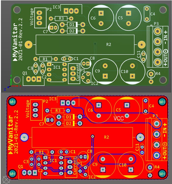
Figure 2, PCB layout of the adjustable power supply circuit (last revision)
The component libraries of a few components were not available in my component libraries storage. So as usual, I used the SamacSys component libraries and installed the missing libraries (schematic symbols, PCB footprint, 3D model) for the IC1[5], IC2[6], IC3[7], and Q1[8]. You have two options to install and use the component libraries. You can either visit the componentsearchengine.com, download and import the libraries in your CAD software or you can use the SamacSys CAD plugins (figure 3). Almost all known electronic designing CAD software are supported [9]. I used Altium Designer, so I installed the component libraries using the Altium plugin [10] (figure 4).

Figure 3, All supported electronic designing CAD software by the SamacSys plugins
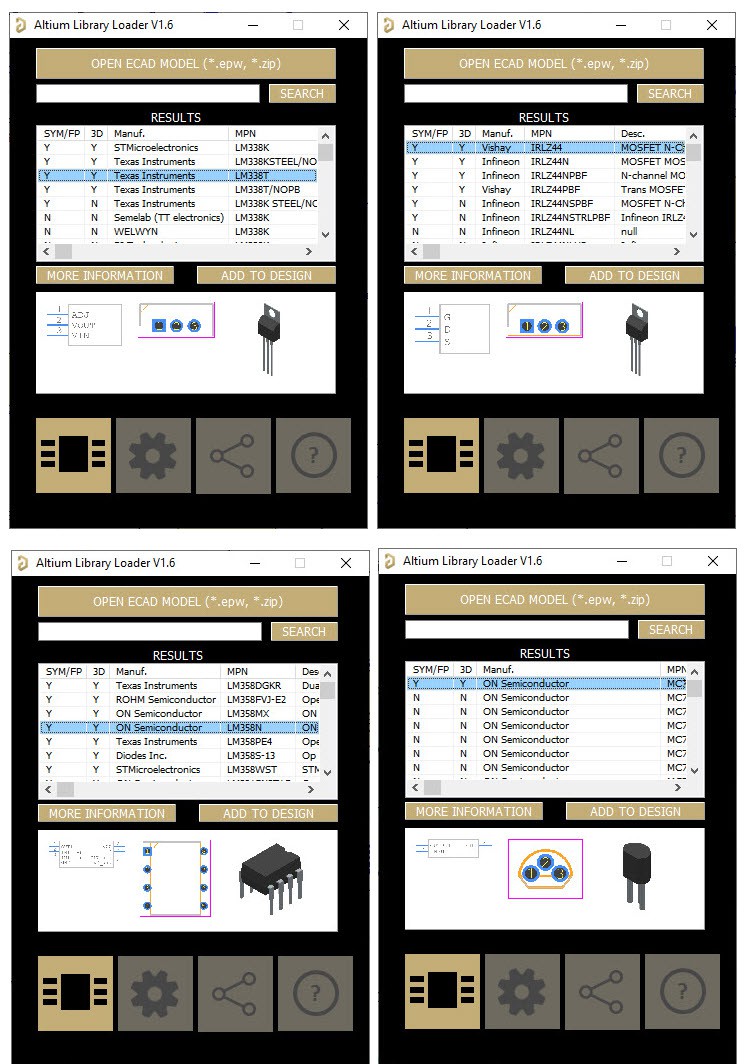
Figure 4, Selected component libraries in the SamacSys Altium plugin
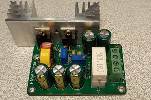
Figure 5 shows the assembled PCB board. The PCBs have been fabricated by the PCBWay in good quality. I did not have any problem with soldering the components at all. The quality of the PCB copper, silkscreen, and solder mask is very good.
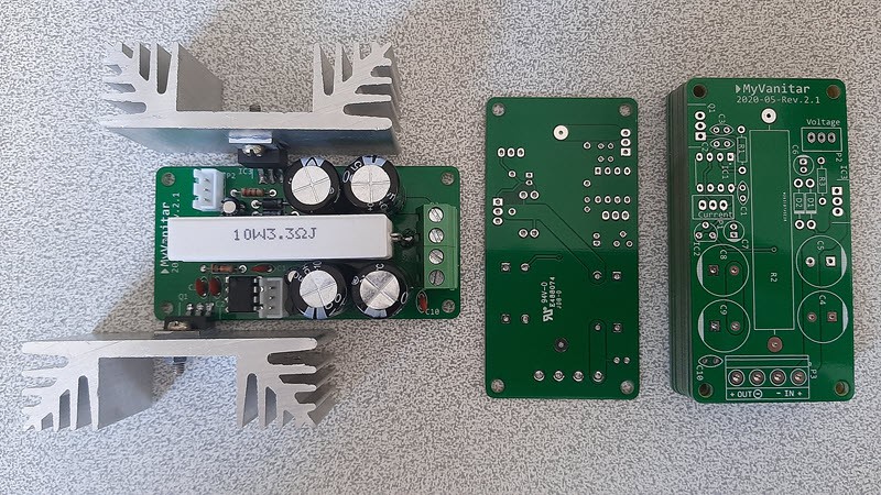
Figure 5, Assembled...
Read more »