 Jelto
JeltoAll components of this build:
- Cal. 30 ammunition case
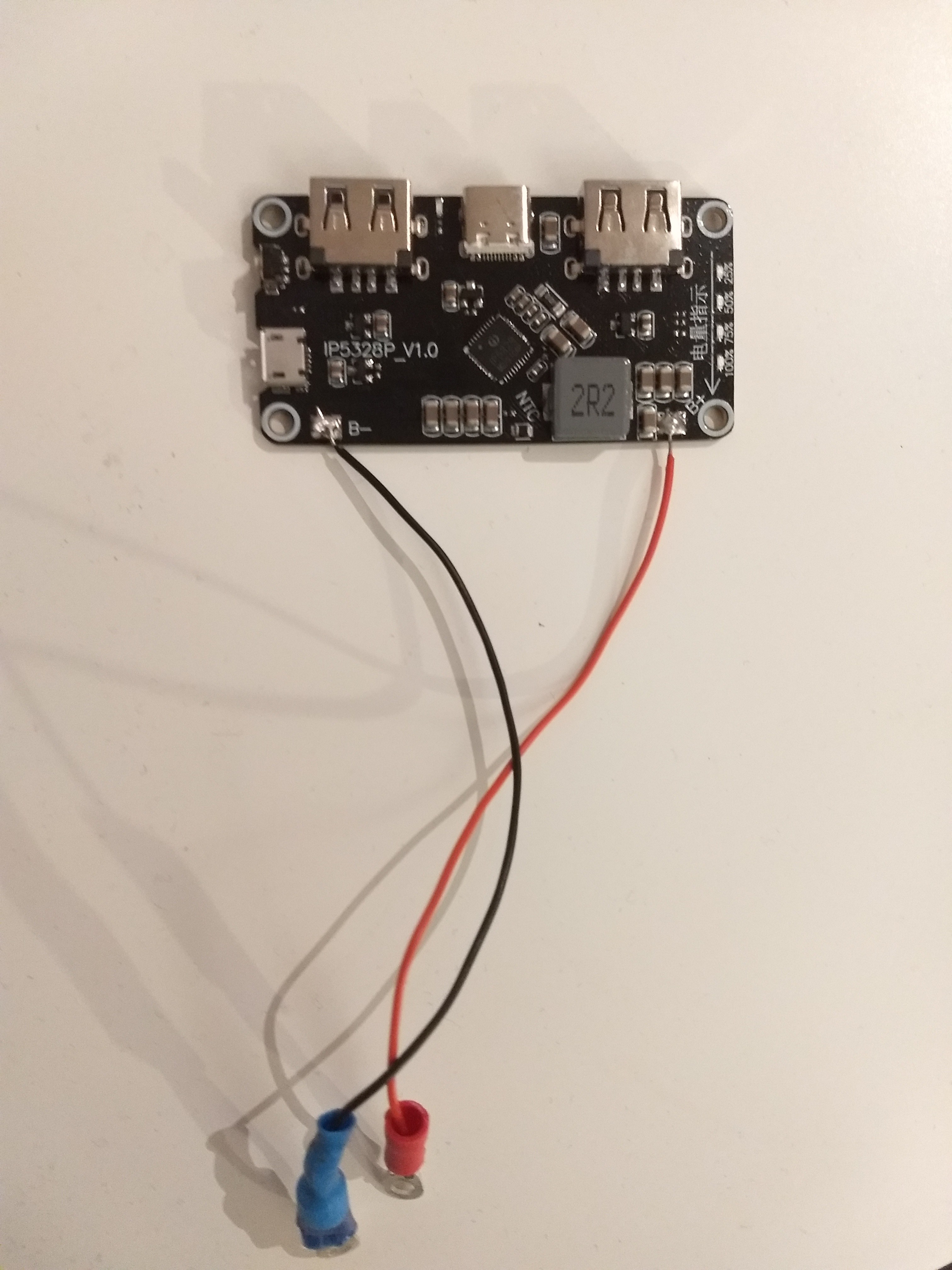
- IP5328P_v1.0 pre build charging circuit from ebay
- 40x 18650 Cells 2AH each
- 5x 18650 4-cell holder from ebay
- 40x Fuse-Holder
- 40x 3A glass fuse
- 80x 20mm M3 spacers
- 5x custom designed PCB
A modular 64Ah power bank from salvaged 18650 cells featuring USB-C (PD, QC, 18watts) to power smartphones and laptops
Already have an account? Log in.
To make the experience fit your profile, pick a username and tell us what interests you.
All components of this build:
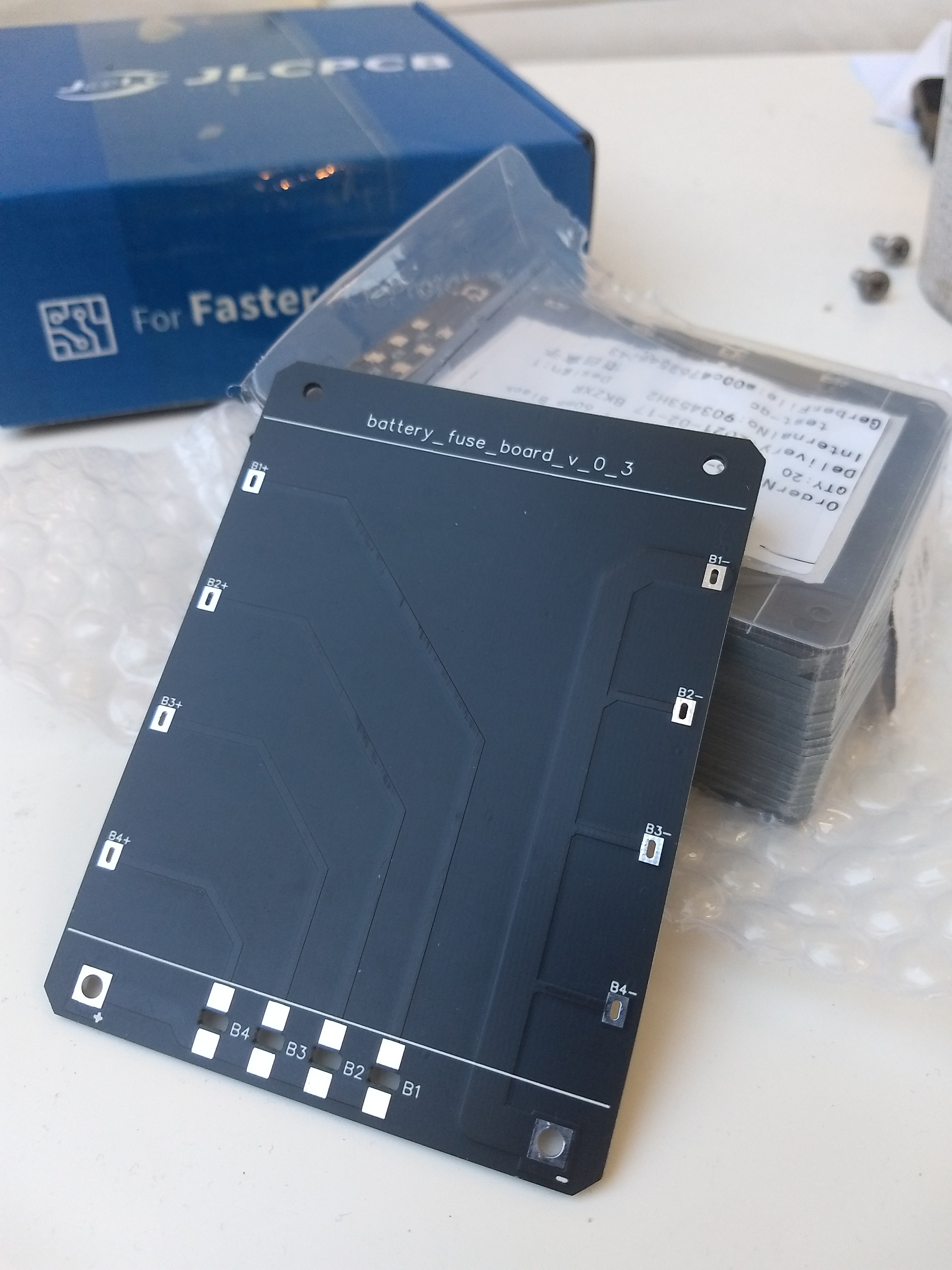
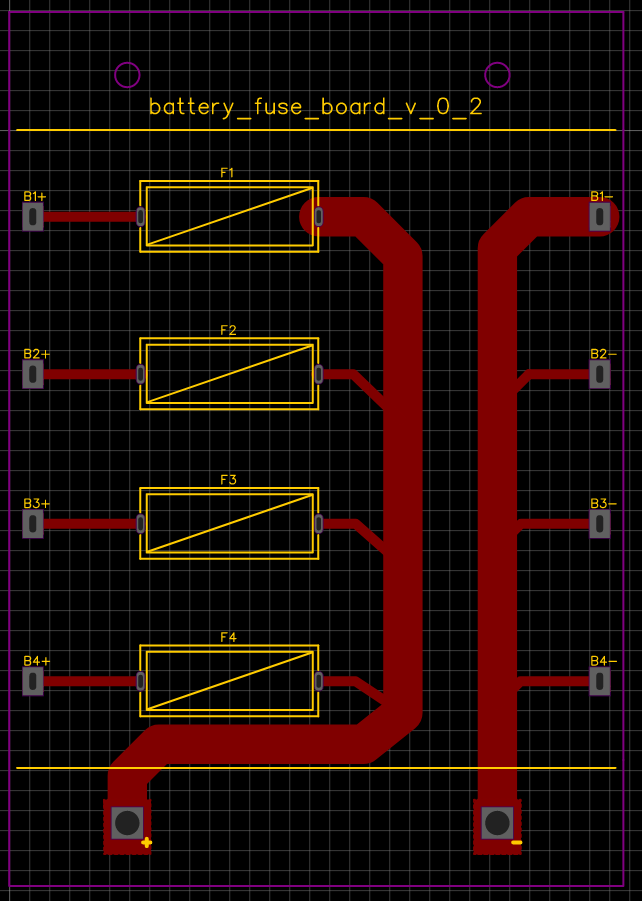
Gerber_battery_fuse_board_v_0_3.zipCurrent v0.3 version of the PCB with fuses build into pcbZip Archive - 10.74 kB - 02/16/2021 at 20:24 |
|
|
Gerber_battery_fuse_board_v_0_2.zipv0.2 version of the PCB with dedicated fuse holdesZip Archive - 9.21 kB - 02/16/2021 at 20:24 |
|
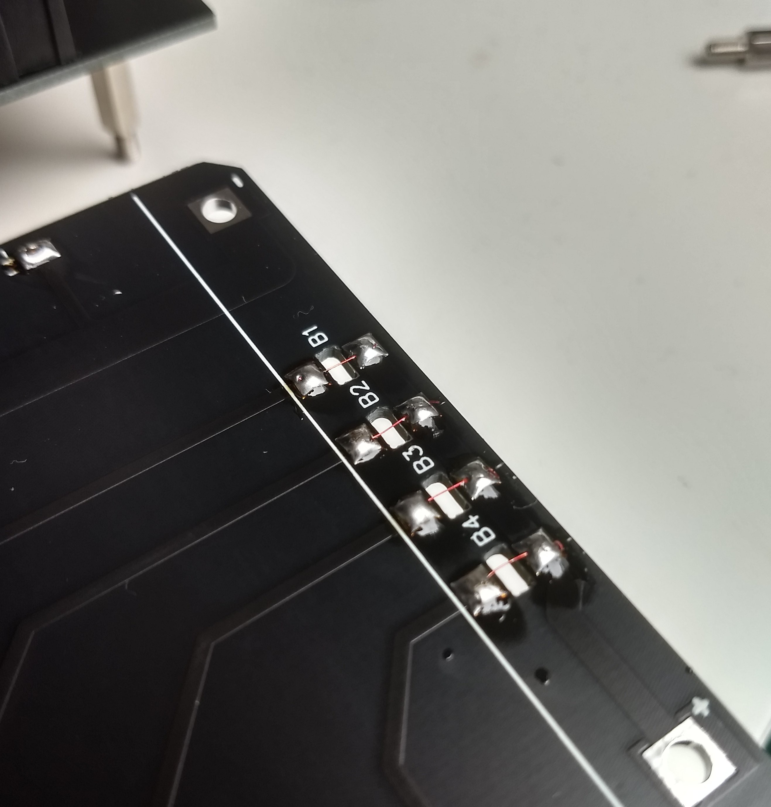
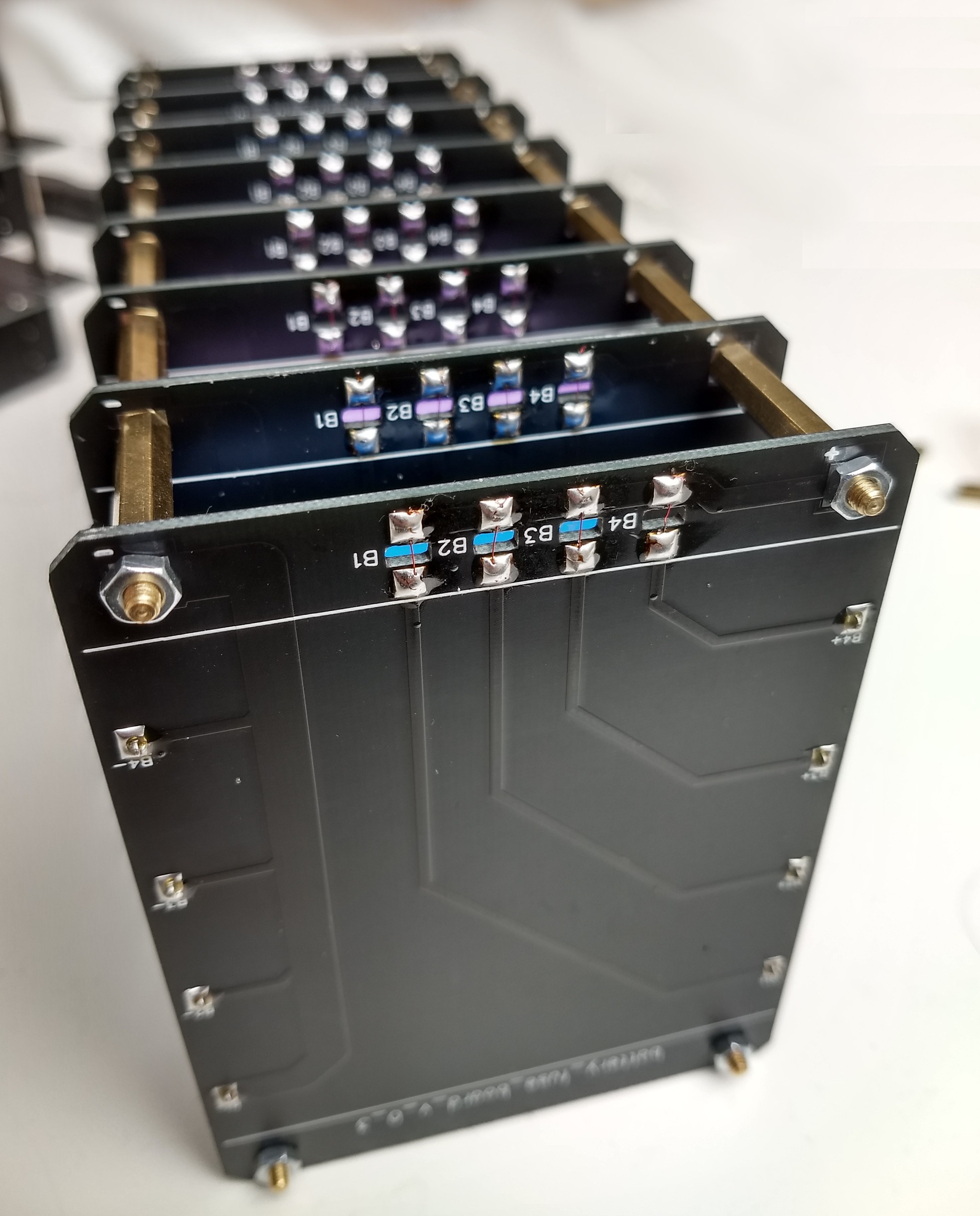
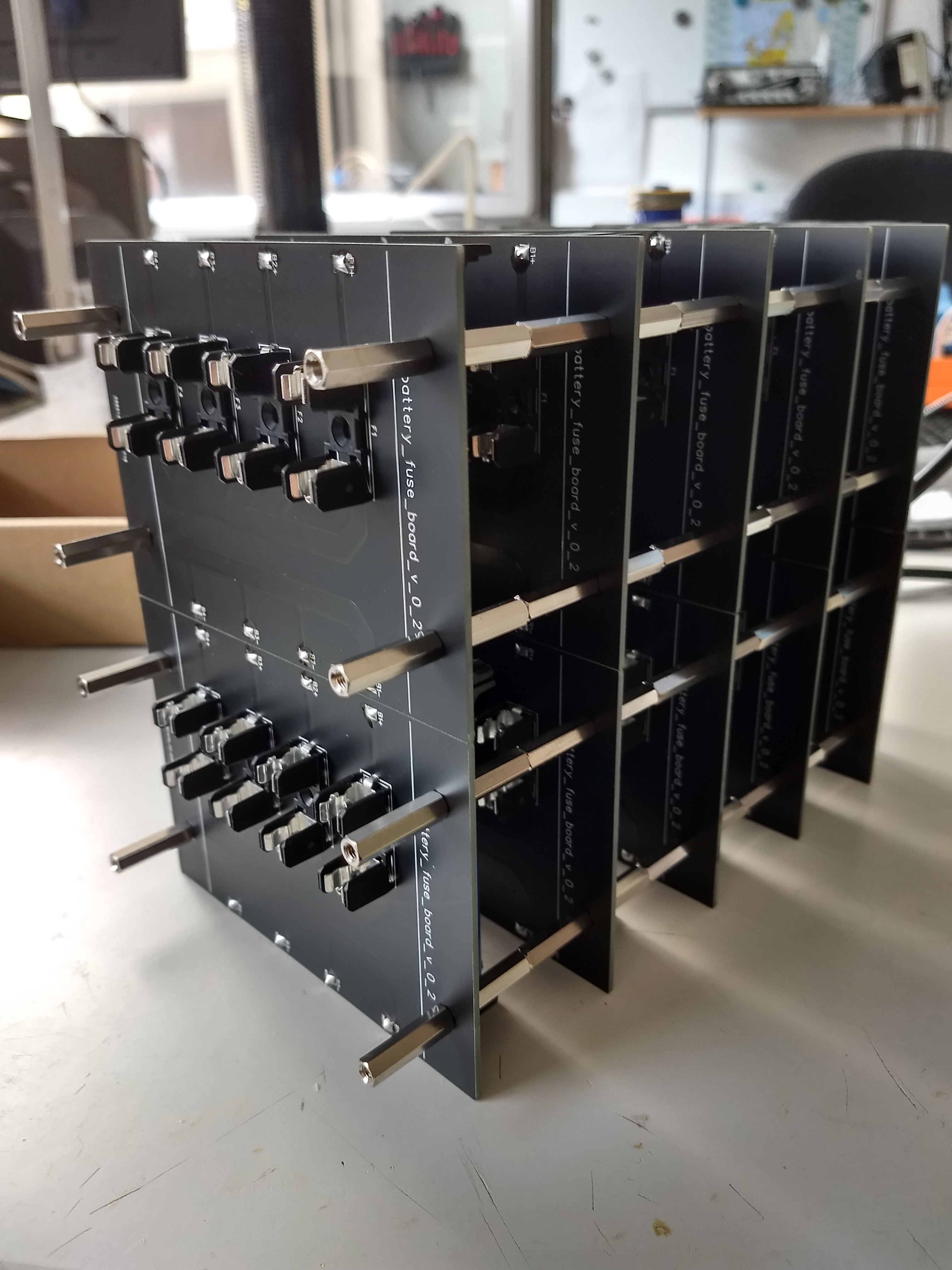
The new PCB version arrived and had to be assembled. The overall assembly process is quite similar to the previous PCB, so I wont go in to too much detail. On each PCB one 18650 4-cell holder has to be mounted. The fuse layout changed a little bit. I removed the dedicated fuse holders and used gaps and solder pads on the PCB itself. So instead of mounting the fuse holders, I soldered thin copper wire bridging the gaps. In the previous step I tested different copper wires and their melting points.
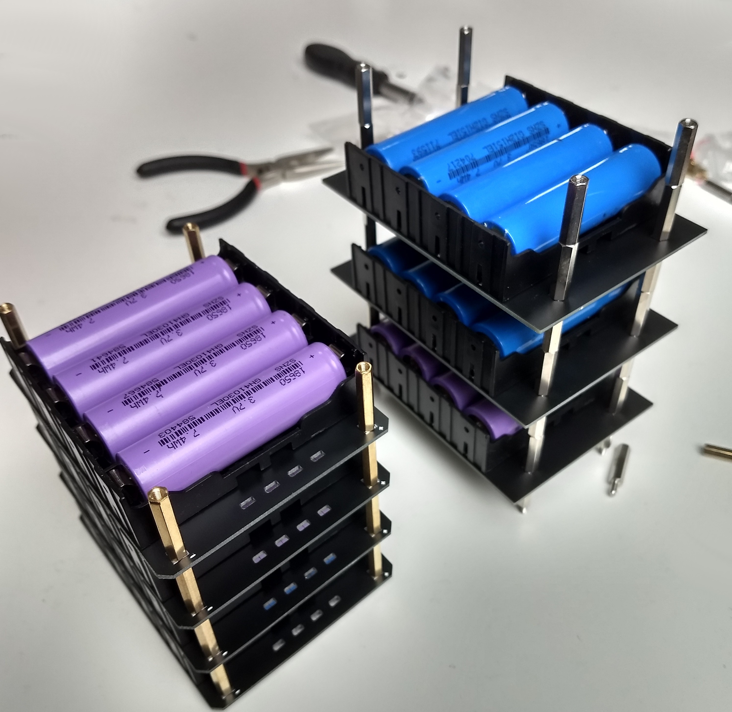
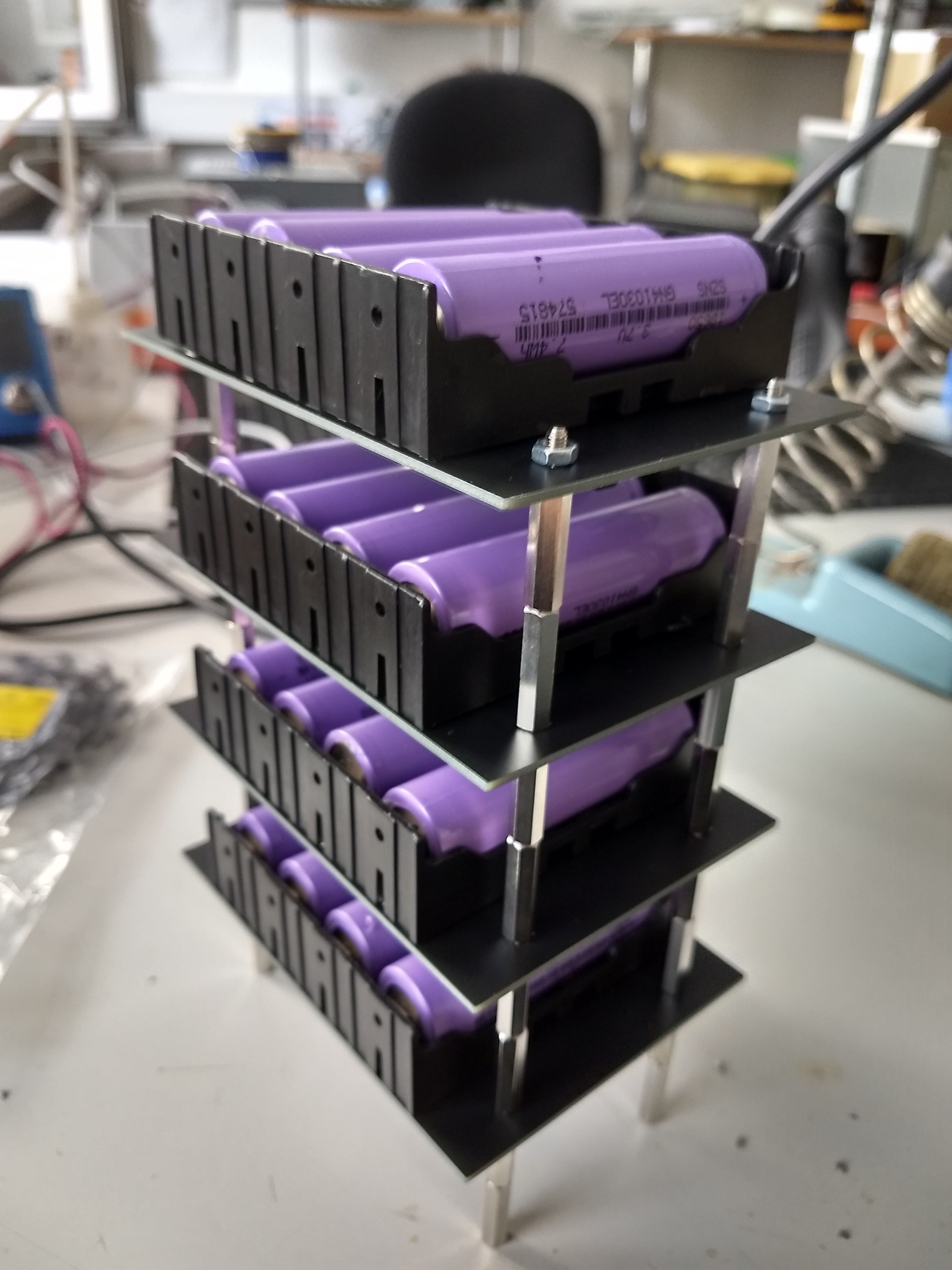
Here is a comparison of v0.3 (left) and v0.2 (right). The general setup is quite similar. Each PCB holds four cells and all PCBs are connected using M3 metal spacers.
However it becomes interesting when we take a look at the height of the stacked PCBs. As I mentioned in the previous post, I wasted quite a lot of space by using dedicated fuse holders on the backside of the PCBs. With the new PCB version you can see that a lot more PCBs can be stacked with the same height!
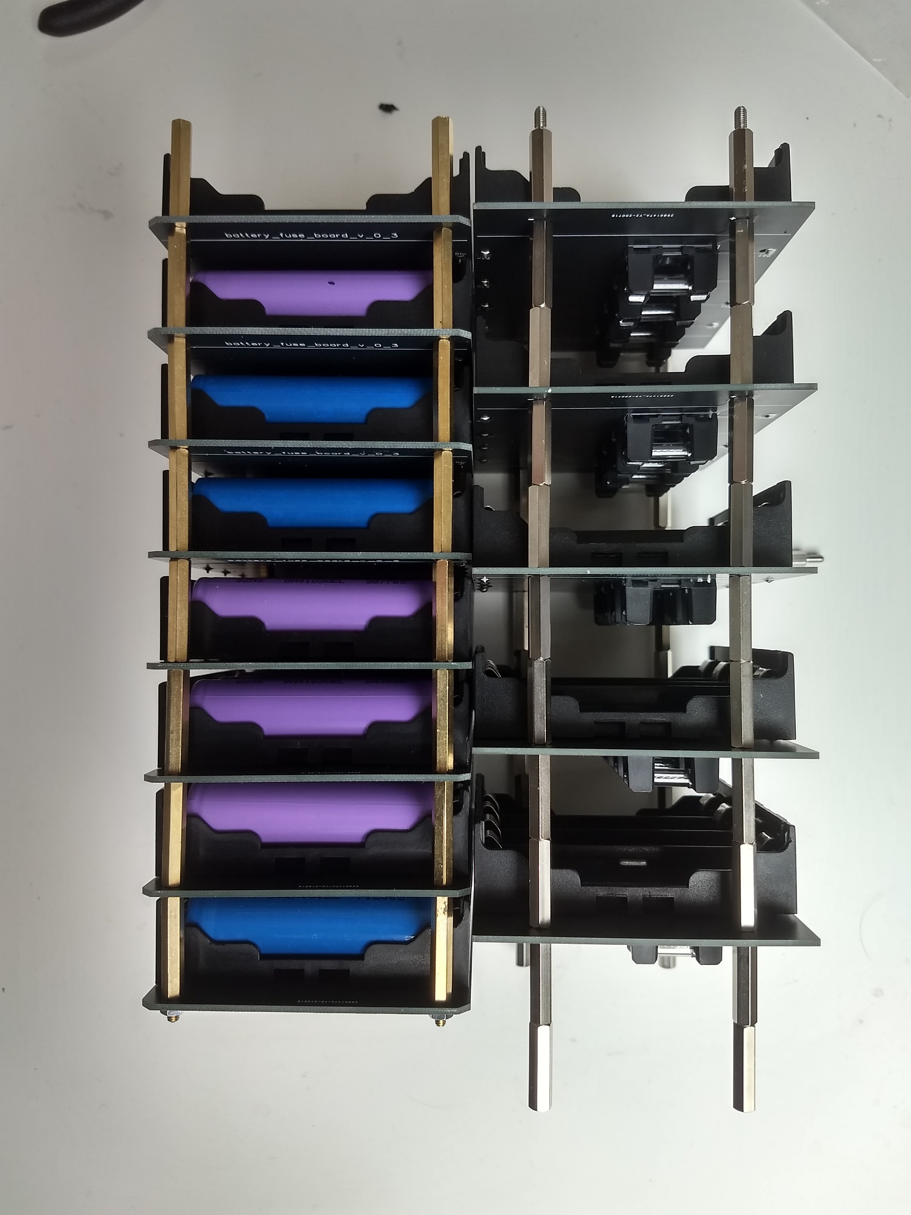
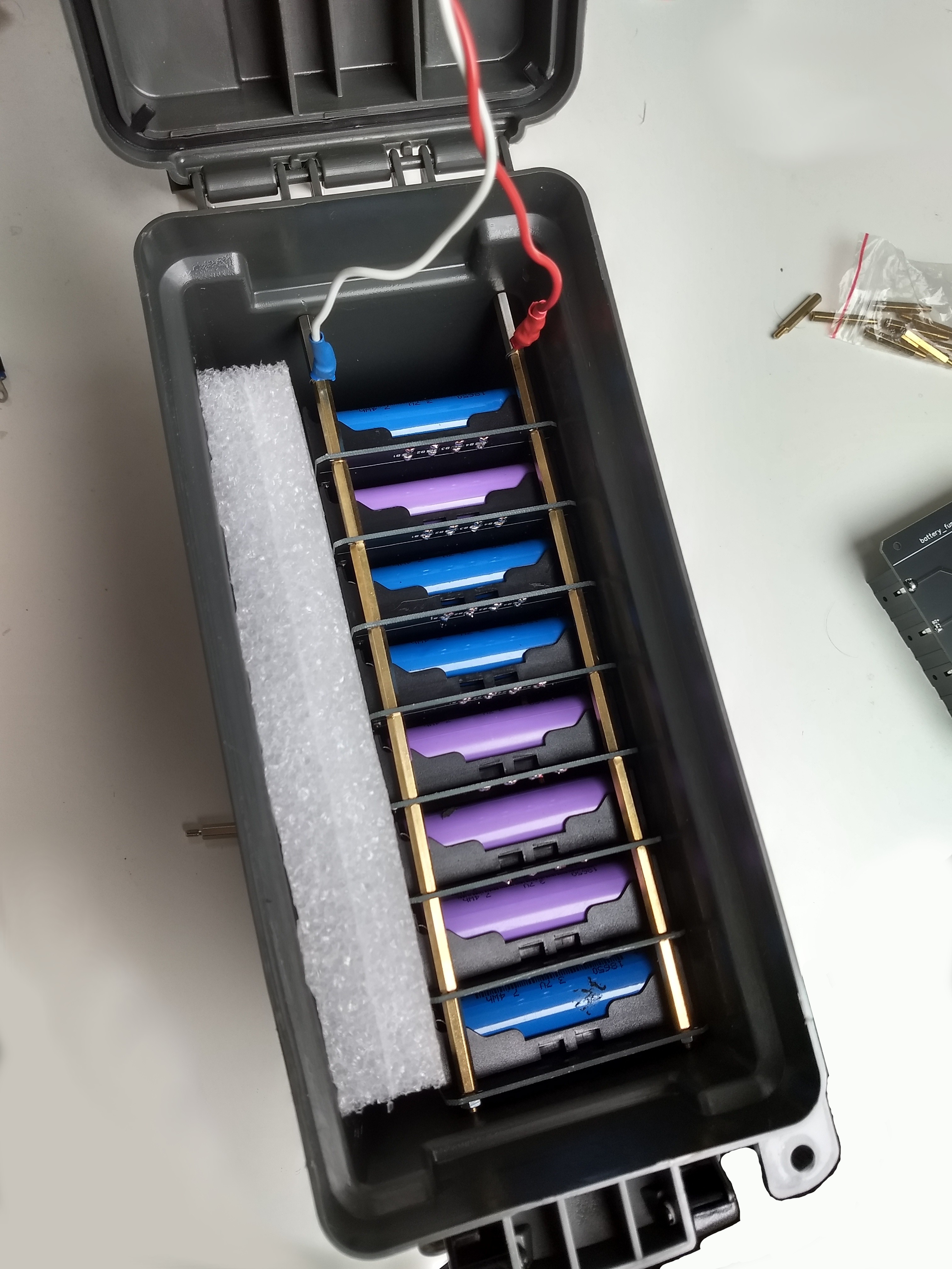
Here the final images of the full pack for the powerbank with eight individual PCBs:
With the height-optimized v0.3 PCB the powerbank has 32 cells in total. The previous PCB only fitted 20 cells in total. This gives around 64Ah of capacity or 236Wh of usable power.
The next steps are to get or design a better charging board which offers more than 18 watts and to build packs with multiple cells in series to get a higher output voltage. But for that the total PCB design has to be changed and will become more complex.
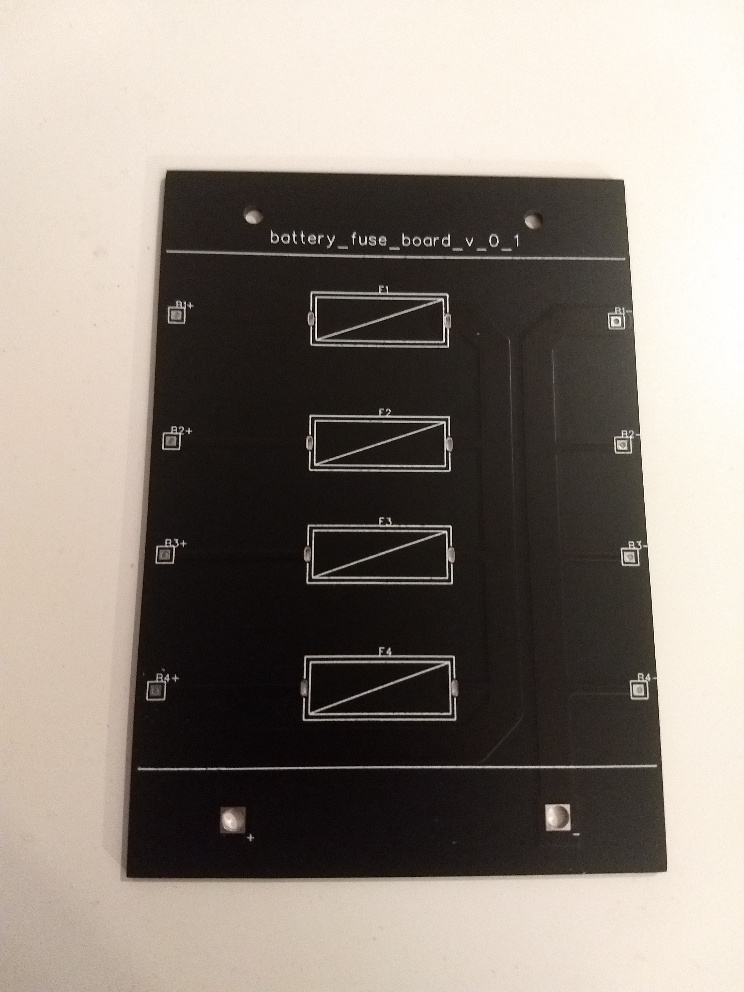
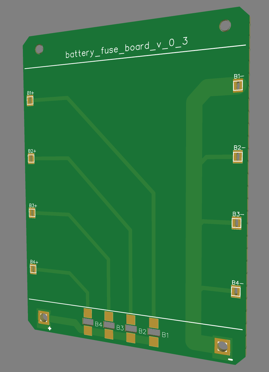
The first improvement of the PCB was about fixing an issue with the size and layout of the board. The second improvement should improve the energy density. The current version is quite bulky with fuses sticking out on the other side of the PCB.
The next version should definitely also have some kind of fuses on board. I like the additional safety especially when mixing old used cells of unknown quality. But putting the fuses on the back wastes a lot of room. I thought about moving the fuse holders on the same side with the cell holders. But this would increase the size of the PCB quite big. Also having four fuse holders and four glass tube fuses per PCB is quite expensive.
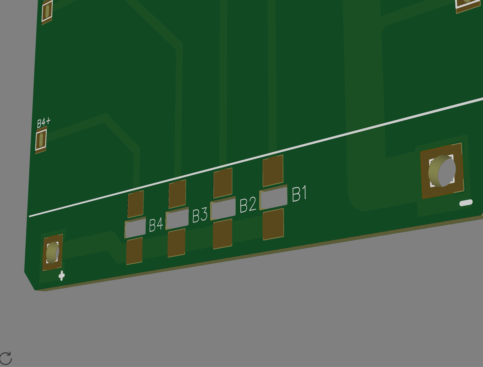
So I came up with another idea. Just build the fuse into the PCB! I also rounded the edges of the PCB. This is mostly a optical improvement but also reduces the physical stress later during assembly.
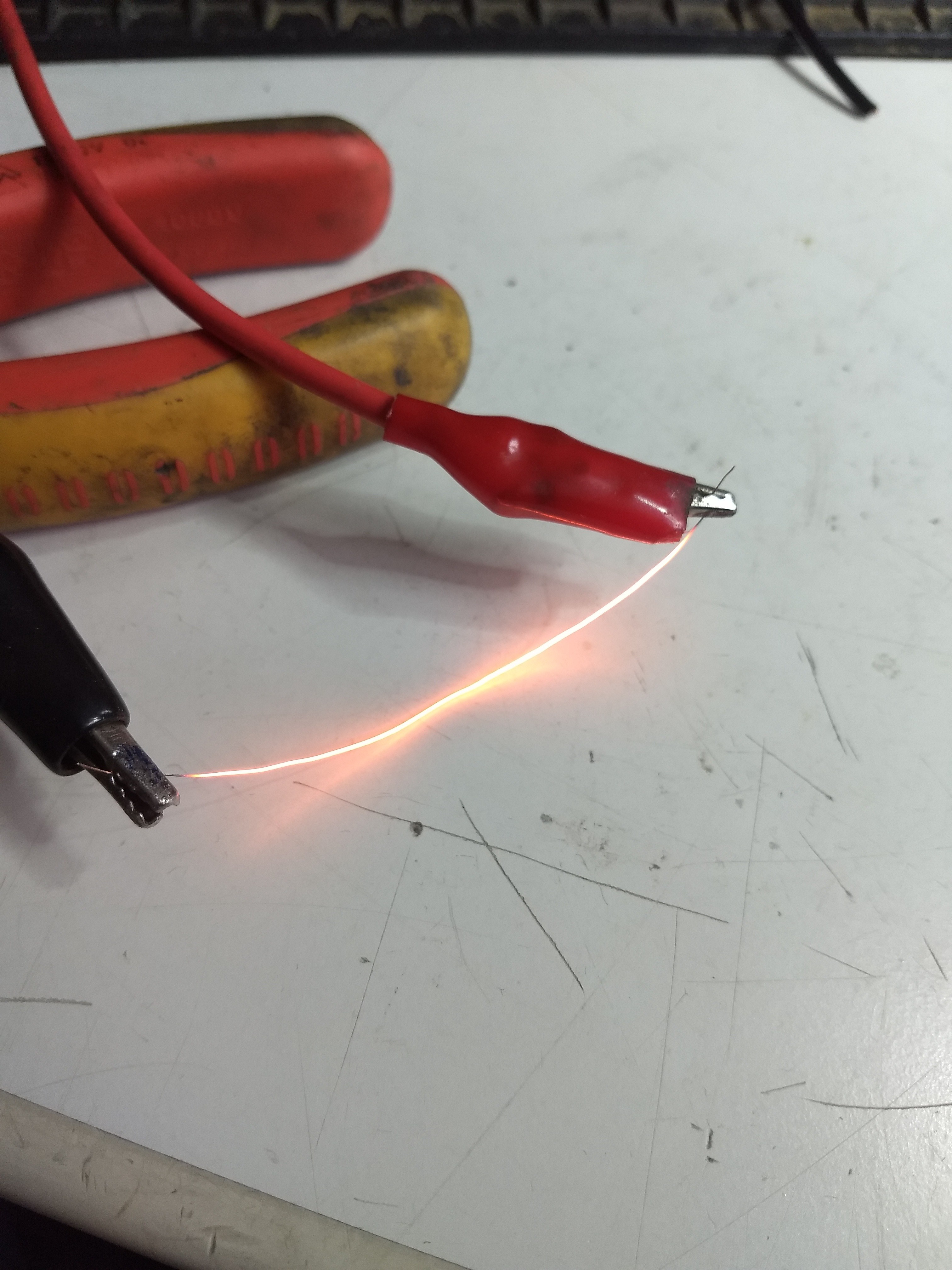
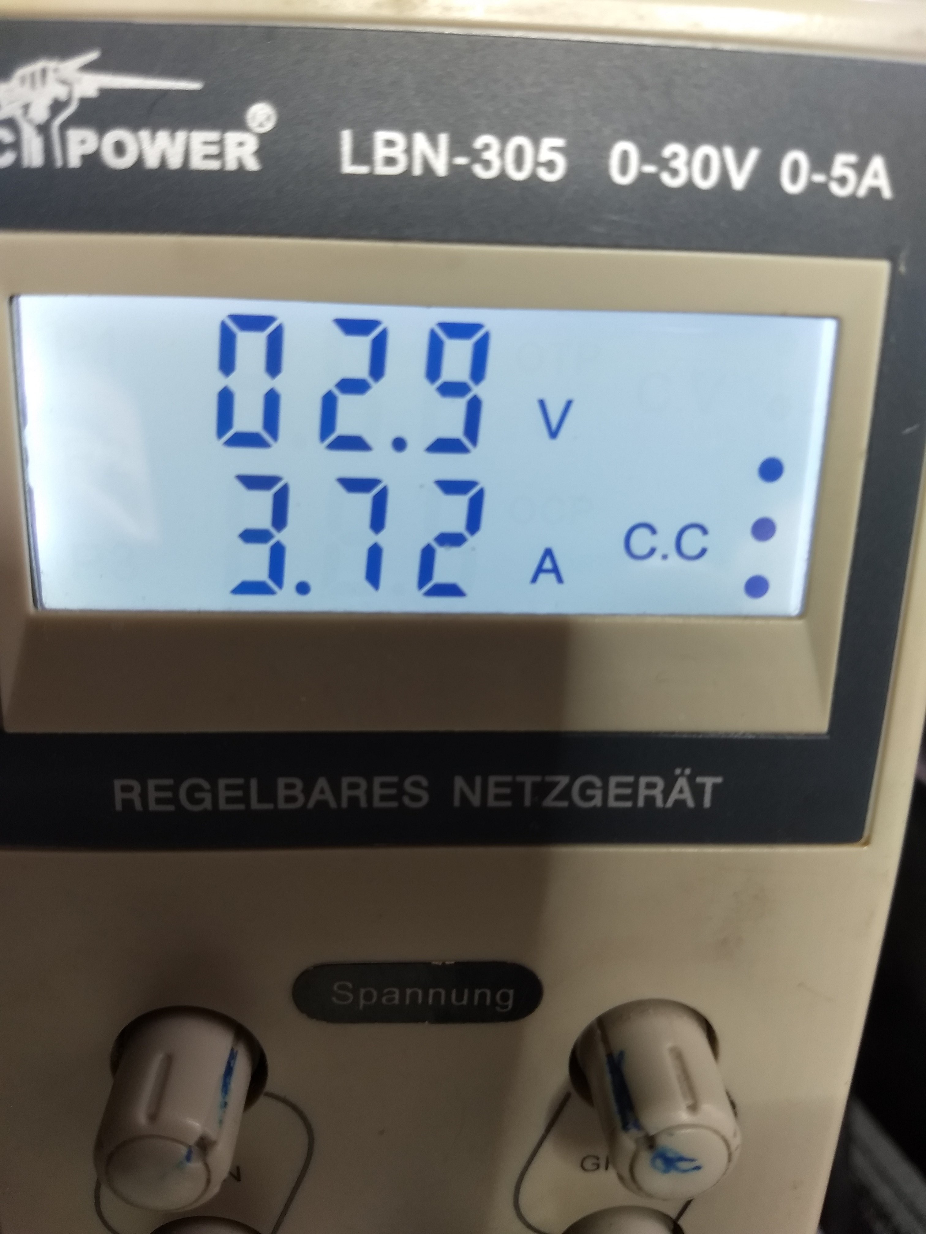
I just added 8 additional solder pads and four gaps in the PCB traces which can be bridged using a very thin wire. The advantage here is that the PCB is not destroyed when you short circuit a cell. In the best case only one wire is melting which can be replaced easily. I added the gap in the PCB to make sure the PCB does not act like a heat sink for the wire and prevents the wire from melting. I've done some tests using a adjustable power supply to find the right size of wire:
I aimed for roughly 4A of maximum current before the wire melts (which is equal to a discharge rate of 2C for the cells, which should be safe)
After some weeks the new PCB version arrived and everything looked fine:
The next step is to connect the cells with each other. This means connecting all four cells on each PCB as well as connecting multiple PCBs with each other.
It is very important to only connect cell with the same voltage/charge!
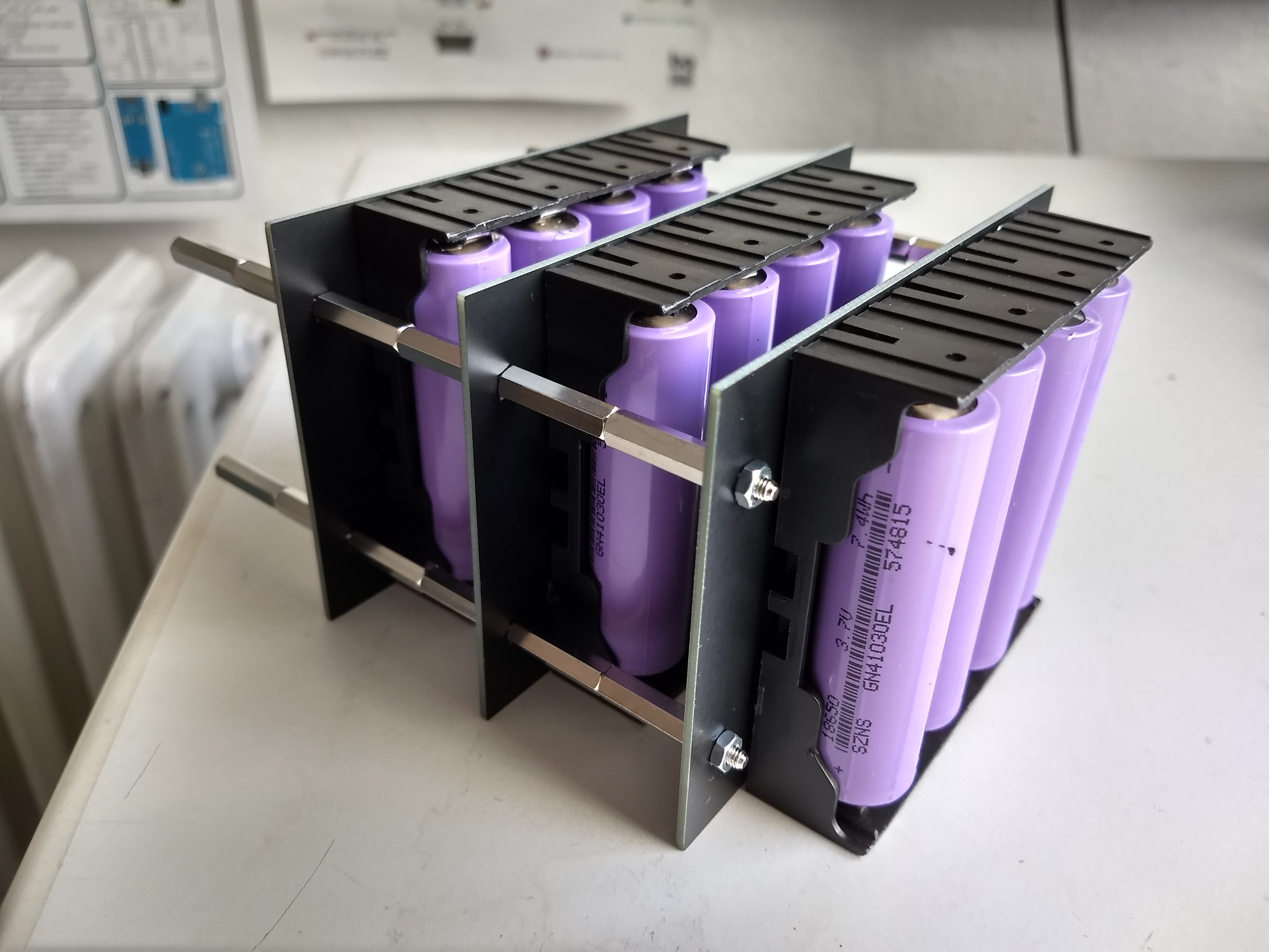
Before connecting the cells, make sure that all cells have the same voltage. I just charged all cells up to 4.2V. The first step was to connect the cells on one PCB. For that I just inserted all the fuses to the fuse holders on each PCB. After populating two PCBs with fuses it was time to stack the first PCBs on top of each other. The electrical connection between both PCBs is done using M3 spacers.
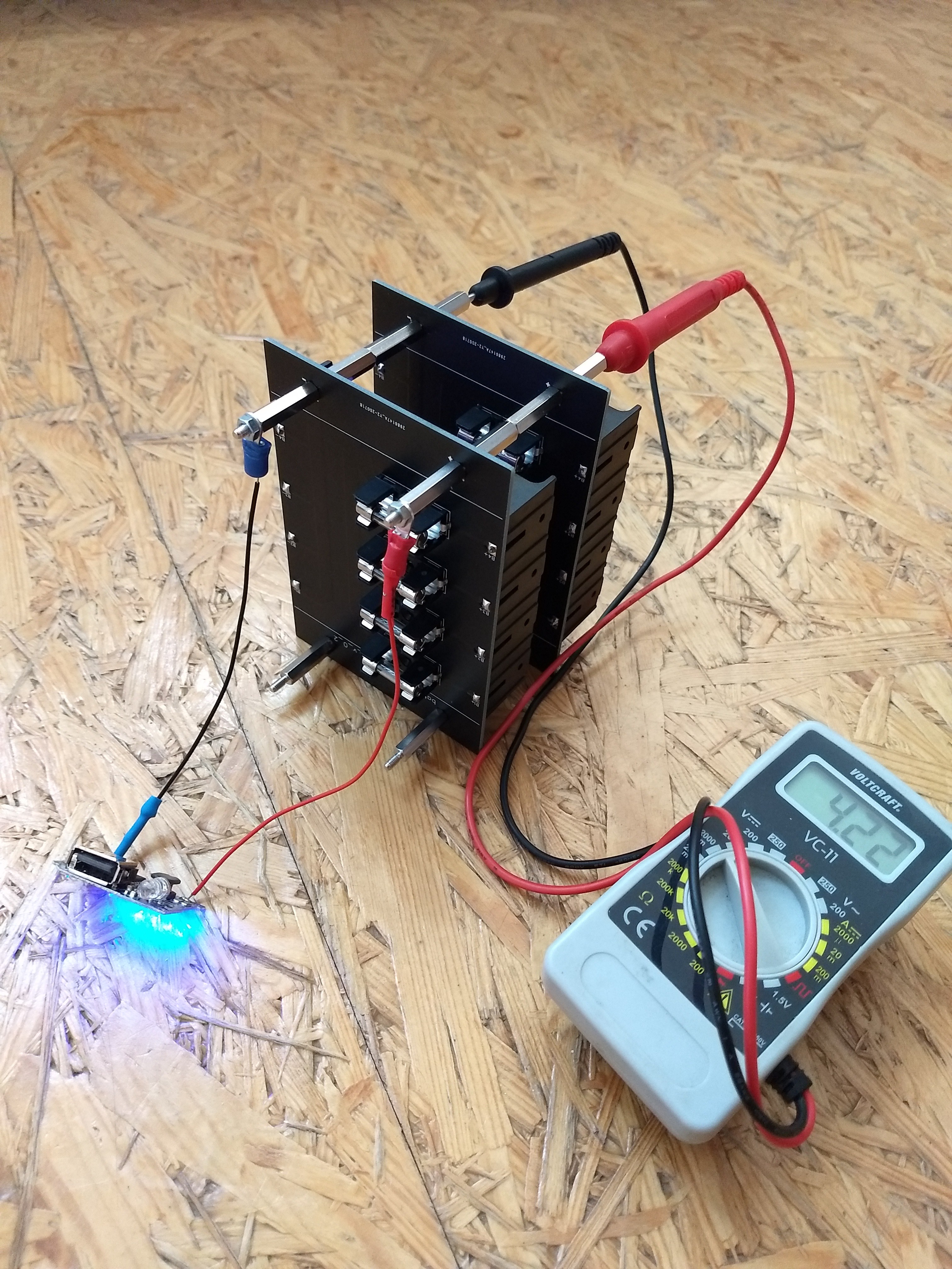
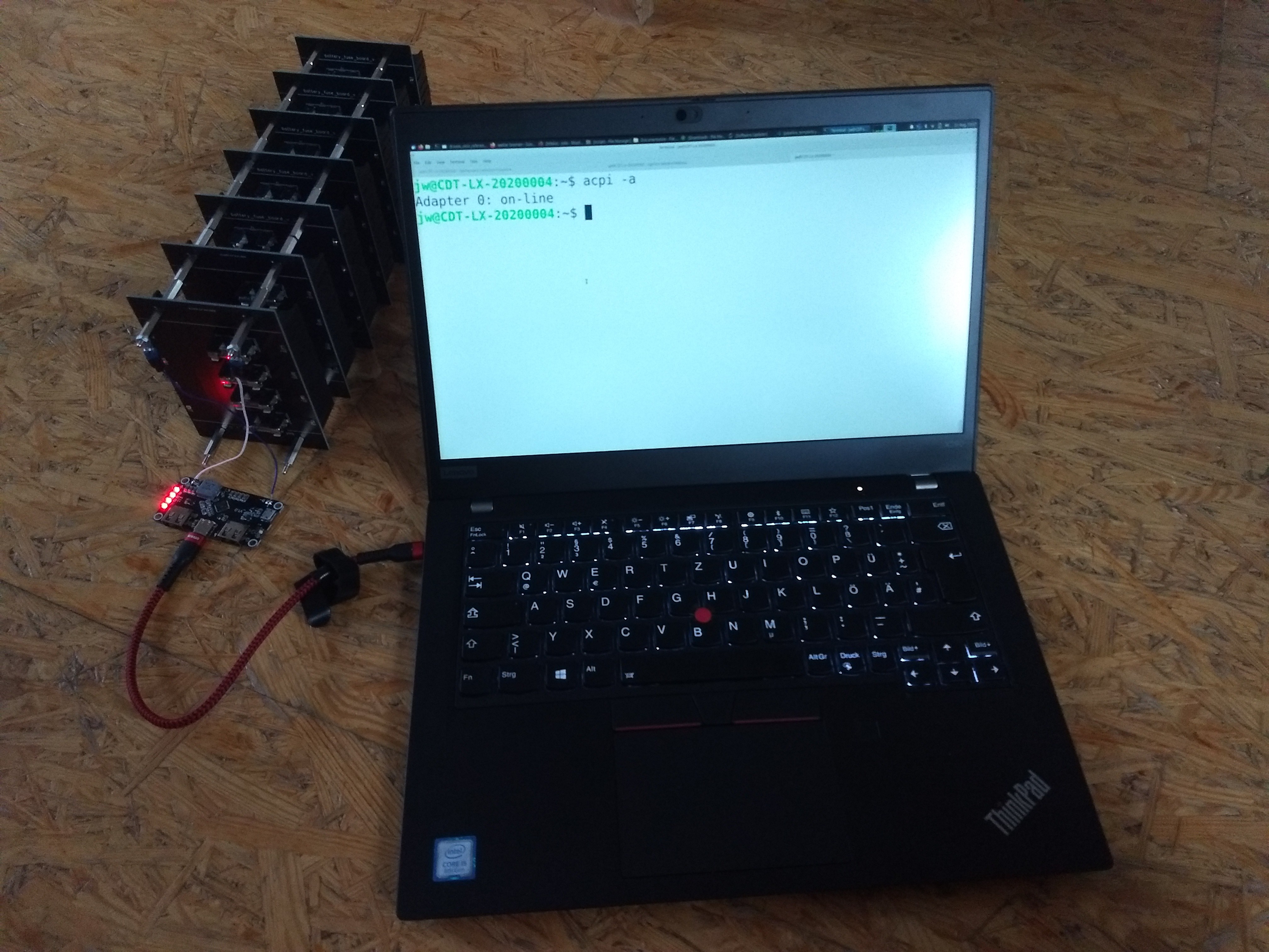
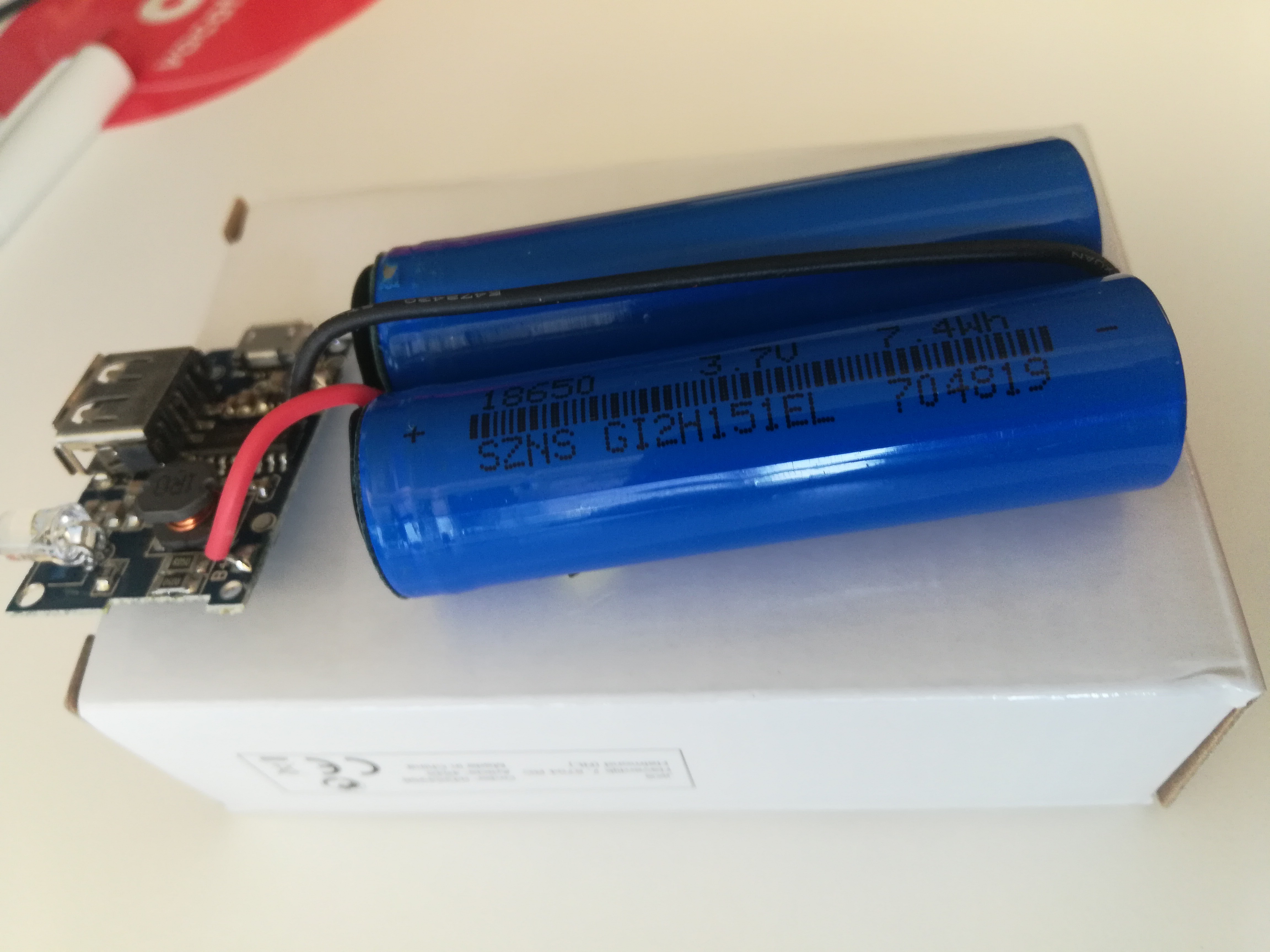
So here you can see the first unit of a working power bank. I added a small USB charging circuit to the Plus and Minus spacers and checked the voltage of the cells using a multi-meter.
I continued adding additional PCBs to the powerbank. Furthermore I changed the USB charging circuit to a more powerful one. The IP5328P can charge using USB-A and USB-C with up to 18 watts (size of the wire was just for testing).
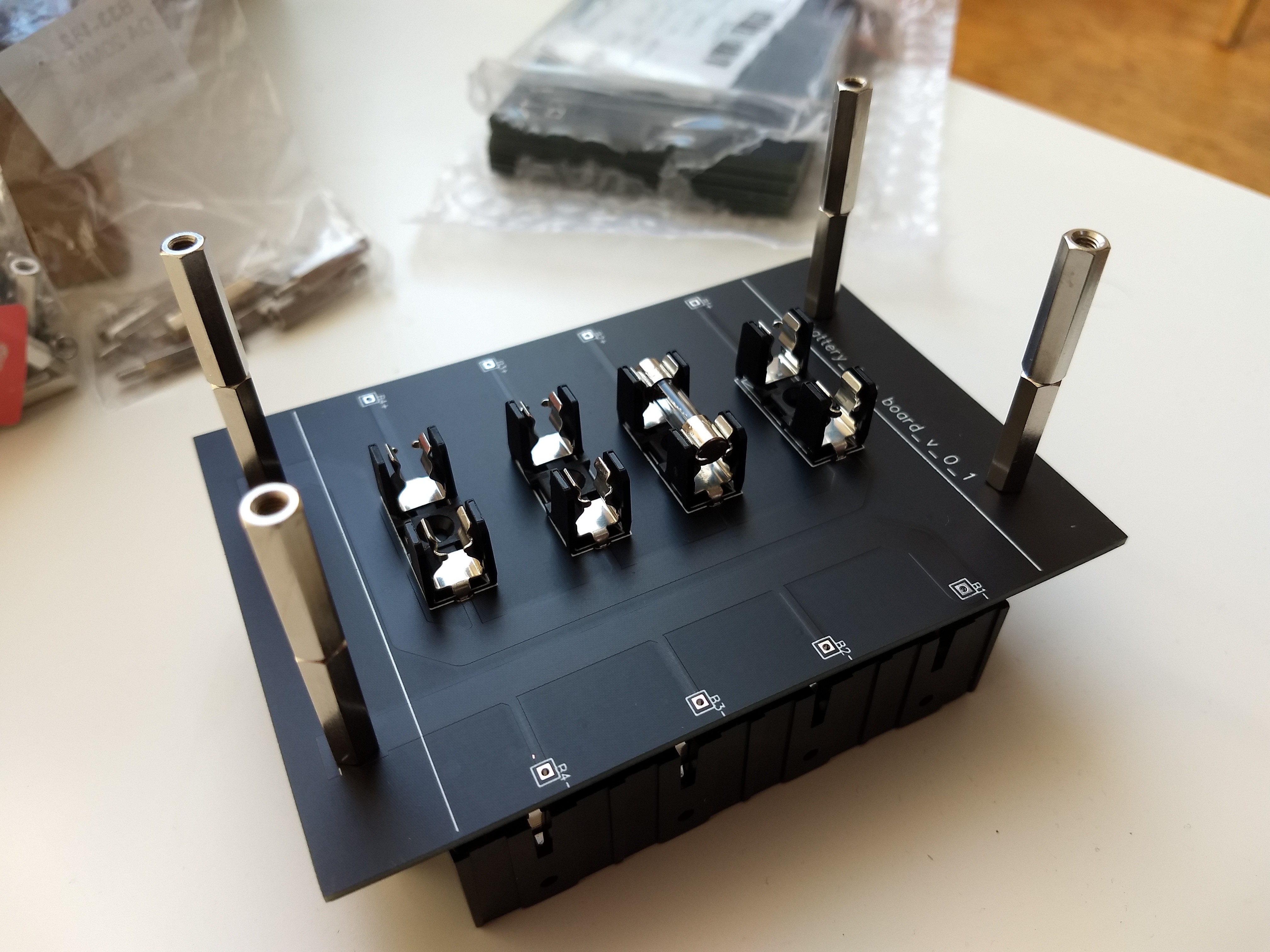
The holes for the 18650 cell holders were to small on the first PCB. So I modified the holes on the PCB and ordered version two from JLCPCB. The PCB gerber files are attached in the project resources.
After receiving the manufactured PCBs I can confirm that all measurements and holes in v0.2 are correct.
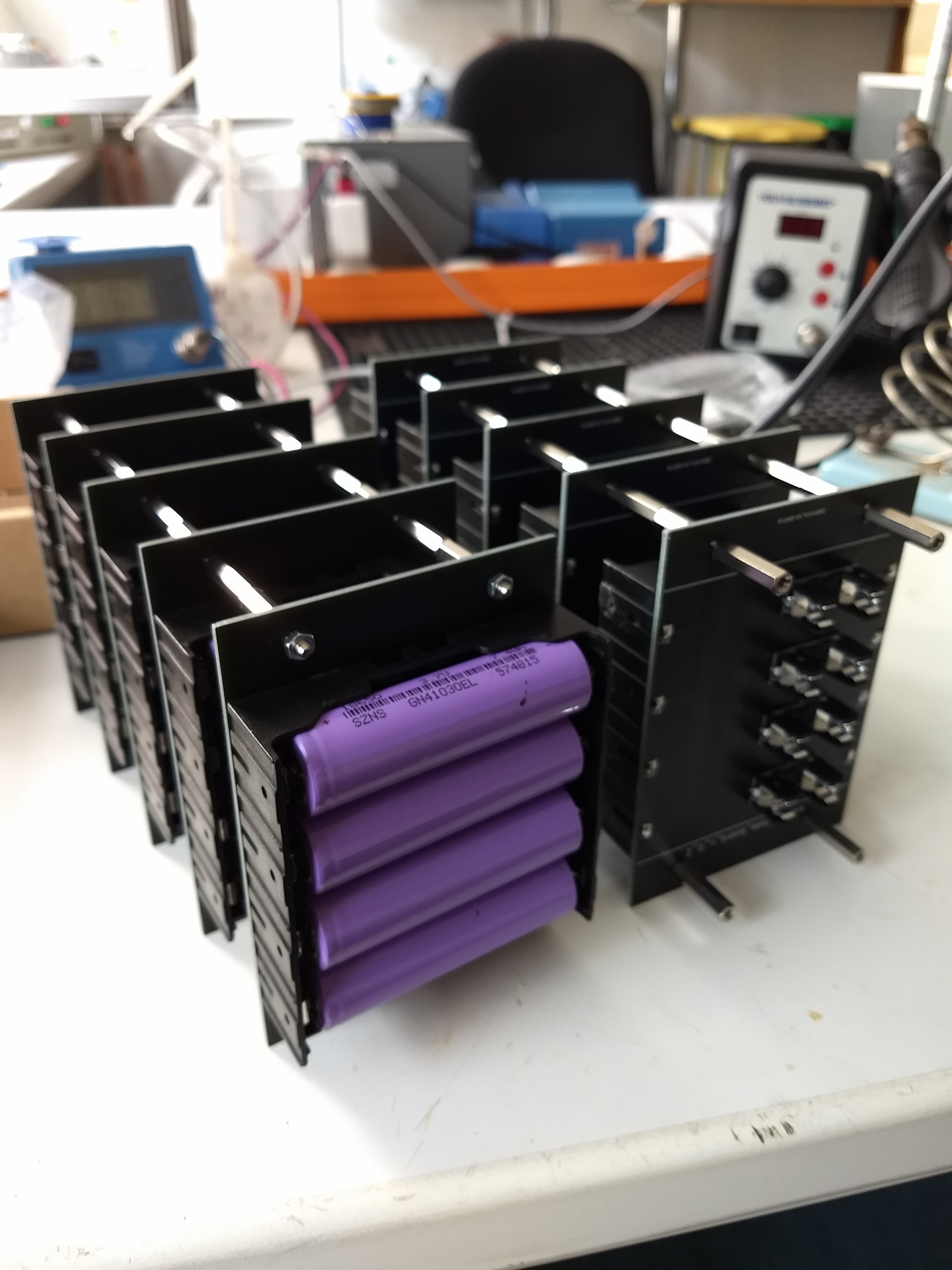
Here is a test-fit of the first three modules stacked together using the metal M3 standoffs. I've continued to populate and solder all ten PCBs. Here are some impressions:
For more safety during the assembly and testing no fuses are used in the modules. In the next step I will charge/balance all cells and connect them electrically.
The first challenge was to think about how to arrange the cells. Requirements from my side were:
With this requirements I decided against just taping all cells together. A way more appealing approach was to design a custom PCB which houses the cells. This PCB can then be used to stack the cells and also to connect them electrically.
For connecting the PCBs I used M3 spacers. The spacers can either be out of metal for a electrical connection or plastic, to isolate (for future designs when doing 2S or 3S cell design). In both cases the spacers give enough structural enforcement for large modules.
So I started a PCB design software, watched some tutorials and created version 1 of the pcb (v2 in the image):
I ordered the PCB from JLCPC. After 2 weeks 10 PCBs arrived. My first lesson in designing PCBs was: measure twice and doublecheck everything! The holes for the 18650 cell holders were way to small!
However the other components fit to the PCB. I've done a test-fit with the fuse holders and the M3 standoffs:
It all stated with a box full of branded powerbanks nobody had any use for. So I started to take a look inside these powerbanks and found what I expeced: brand new useful 18650 cells! Each cell has a rated capacity of 2AH or 7.4Wh. Tests show that all of the cells had around 2AH capacity.
So I gathered some friends to help me disassemble and salvage all of the cells. We rescued 38 cells in total!
[this comment has been deleted]


I've got a bunch of old modem batteries sitting around my shop waiting for a project like this. Thanks for the inspiration!
Using old modem batteries for the powerbank is quite a good idea! Make sure to check the next version of my build. I have a new PCB version in progress which doesn't use the full size fuse-holders but instead it uses replaceable copper wires on the PCB. This design reduces the cost and size per board a lot.

 Hendra Kusumah
 mbsg99
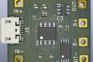
 Abduulah Omran
Hey
in the current version all cells are connected in parallel and the PCB is just doing the electrical connection. You can only add and remove cells if the have the exact same voltage/charge otherwise you will blow a fuse or damage the board/cells.
I would love to add more logic to the board in the future so that you are able to add and remove cells on demand and also build a powerbank with 8 volts or 12 volts.
But this is something for the next versions ;)