 Jelto
JeltoThe first improvement of the PCB was about fixing an issue with the size and layout of the board. The second improvement should improve the energy density. The current version is quite bulky with fuses sticking out on the other side of the PCB.
The next version should definitely also have some kind of fuses on board. I like the additional safety especially when mixing old used cells of unknown quality. But putting the fuses on the back wastes a lot of room. I thought about moving the fuse holders on the same side with the cell holders. But this would increase the size of the PCB quite big. Also having four fuse holders and four glass tube fuses per PCB is quite expensive.
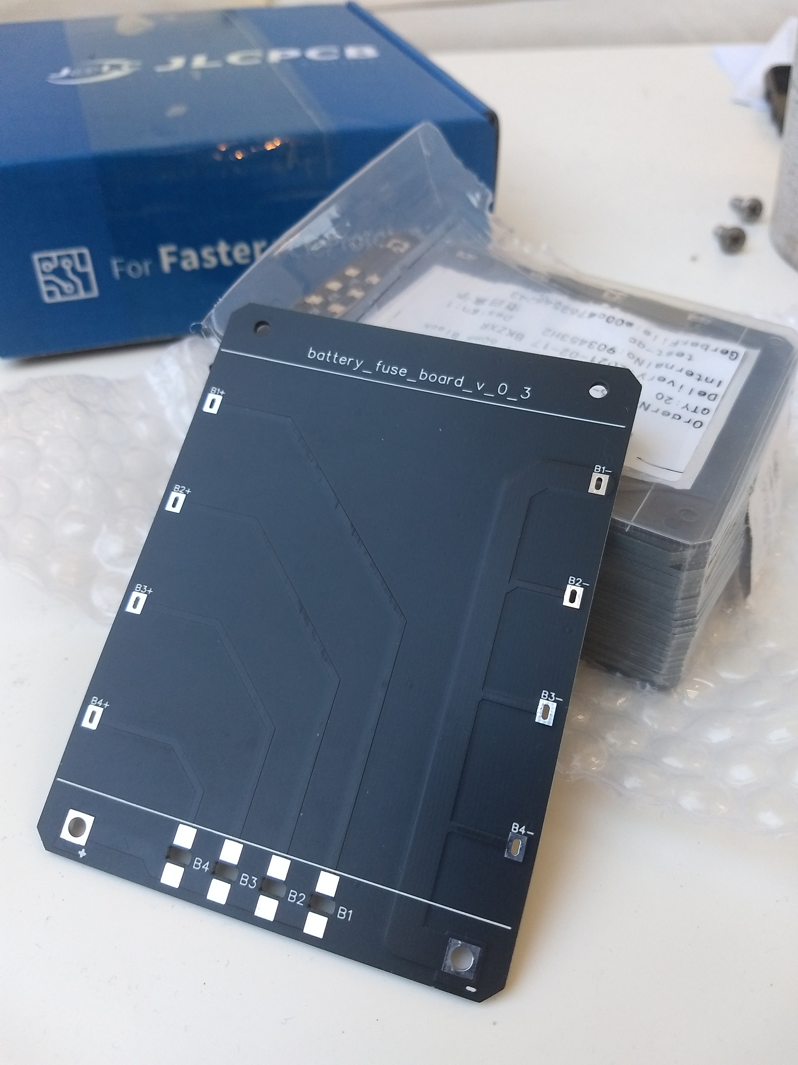
So I came up with another idea. Just build the fuse into the PCB! I also rounded the edges of the PCB. This is mostly a optical improvement but also reduces the physical stress later during assembly.
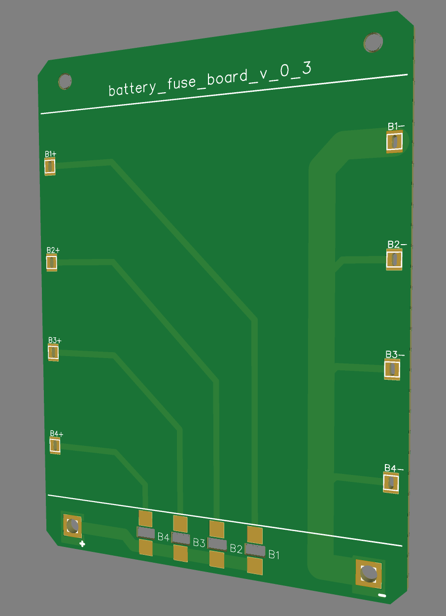
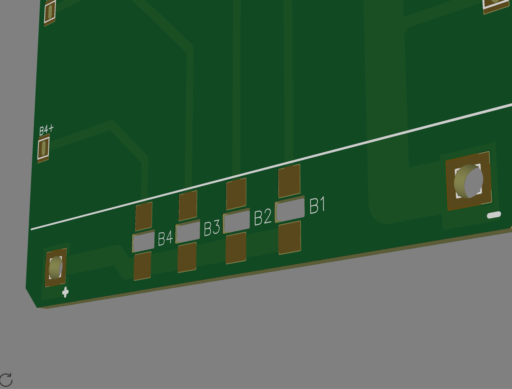
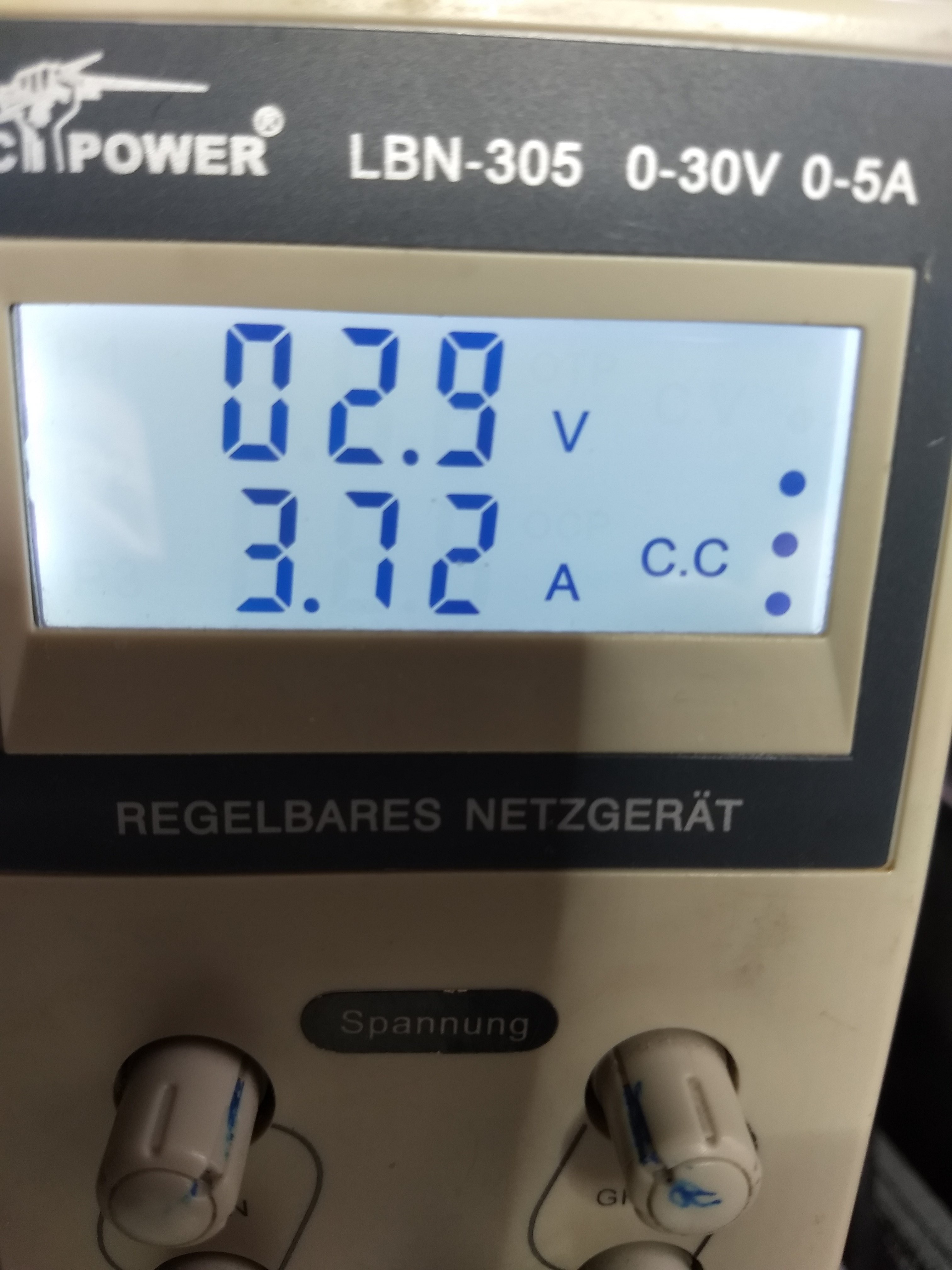
I just added 8 additional solder pads and four gaps in the PCB traces which can be bridged using a very thin wire. The advantage here is that the PCB is not destroyed when you short circuit a cell. In the best case only one wire is melting which can be replaced easily. I added the gap in the PCB to make sure the PCB does not act like a heat sink for the wire and prevents the wire from melting. I've done some tests using a adjustable power supply to find the right size of wire:
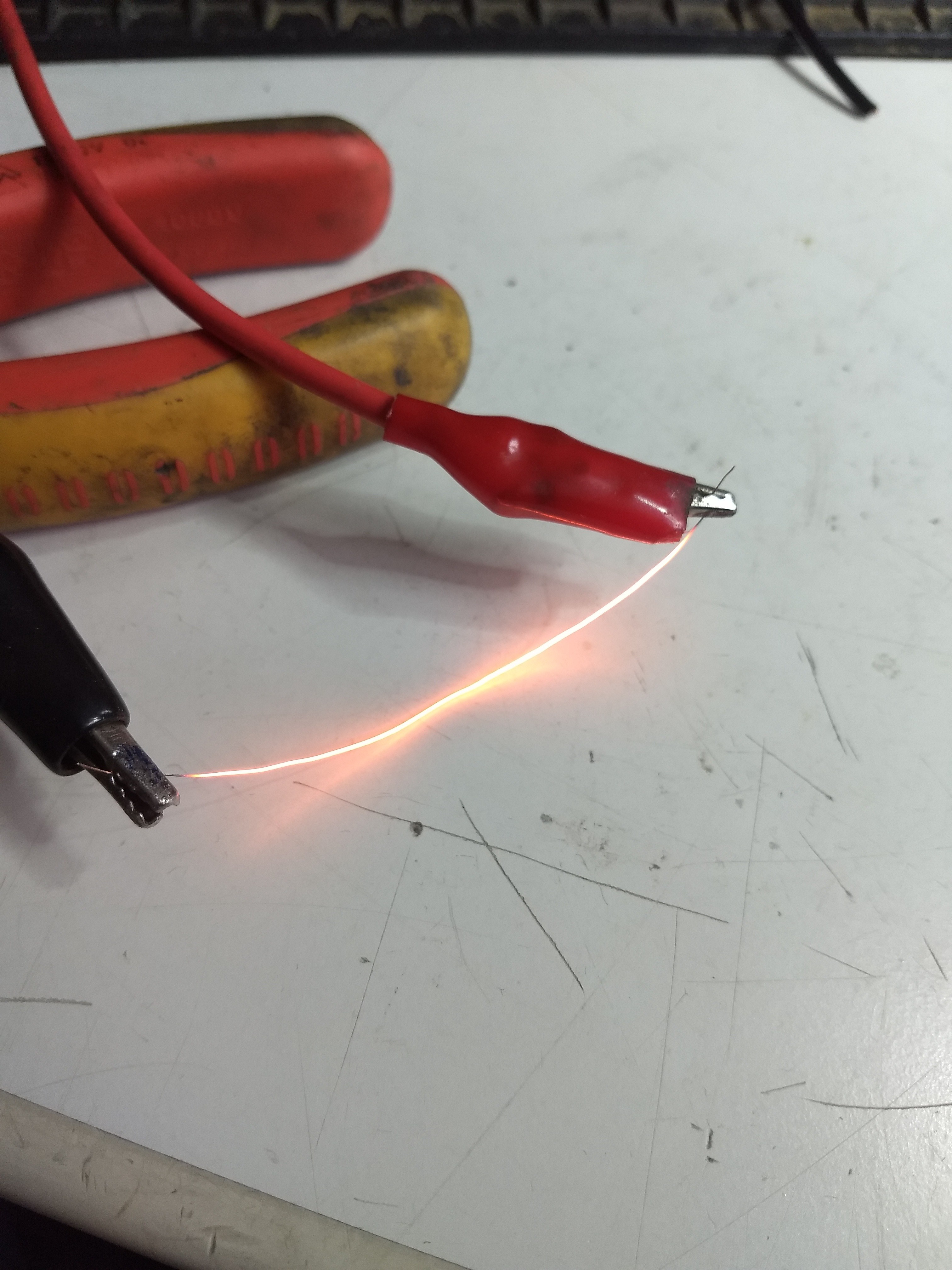
I aimed for roughly 4A of maximum current before the wire melts (which is equal to a discharge rate of 2C for the cells, which should be safe)
After some weeks the new PCB version arrived and everything looked fine:
Discussions
Become a Hackaday.io Member
Create an account to leave a comment. Already have an account? Log In.