 Jelto
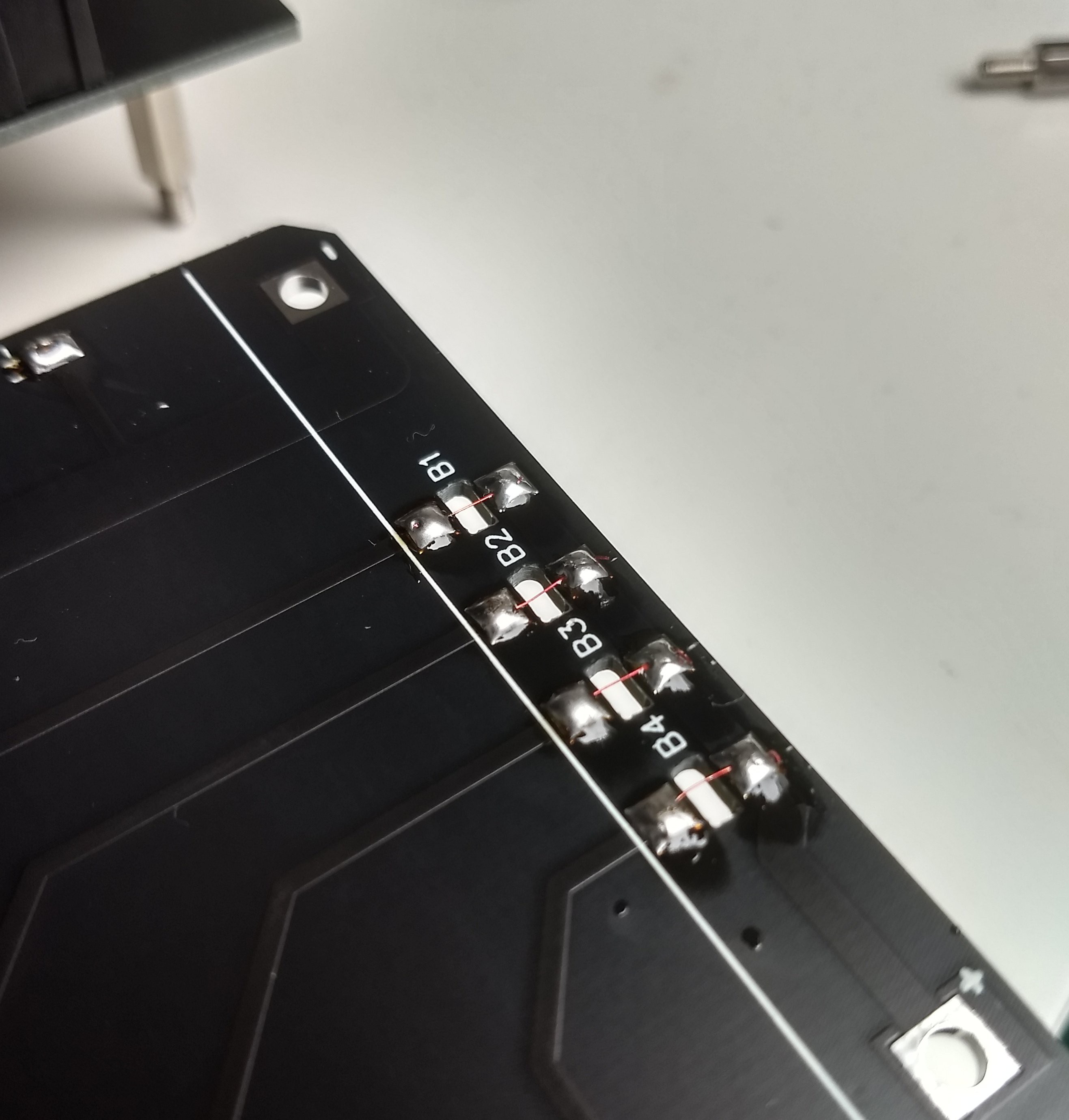
JeltoThe new PCB version arrived and had to be assembled. The overall assembly process is quite similar to the previous PCB, so I wont go in to too much detail. On each PCB one 18650 4-cell holder has to be mounted. The fuse layout changed a little bit. I removed the dedicated fuse holders and used gaps and solder pads on the PCB itself. So instead of mounting the fuse holders, I soldered thin copper wire bridging the gaps. In the previous step I tested different copper wires and their melting points.
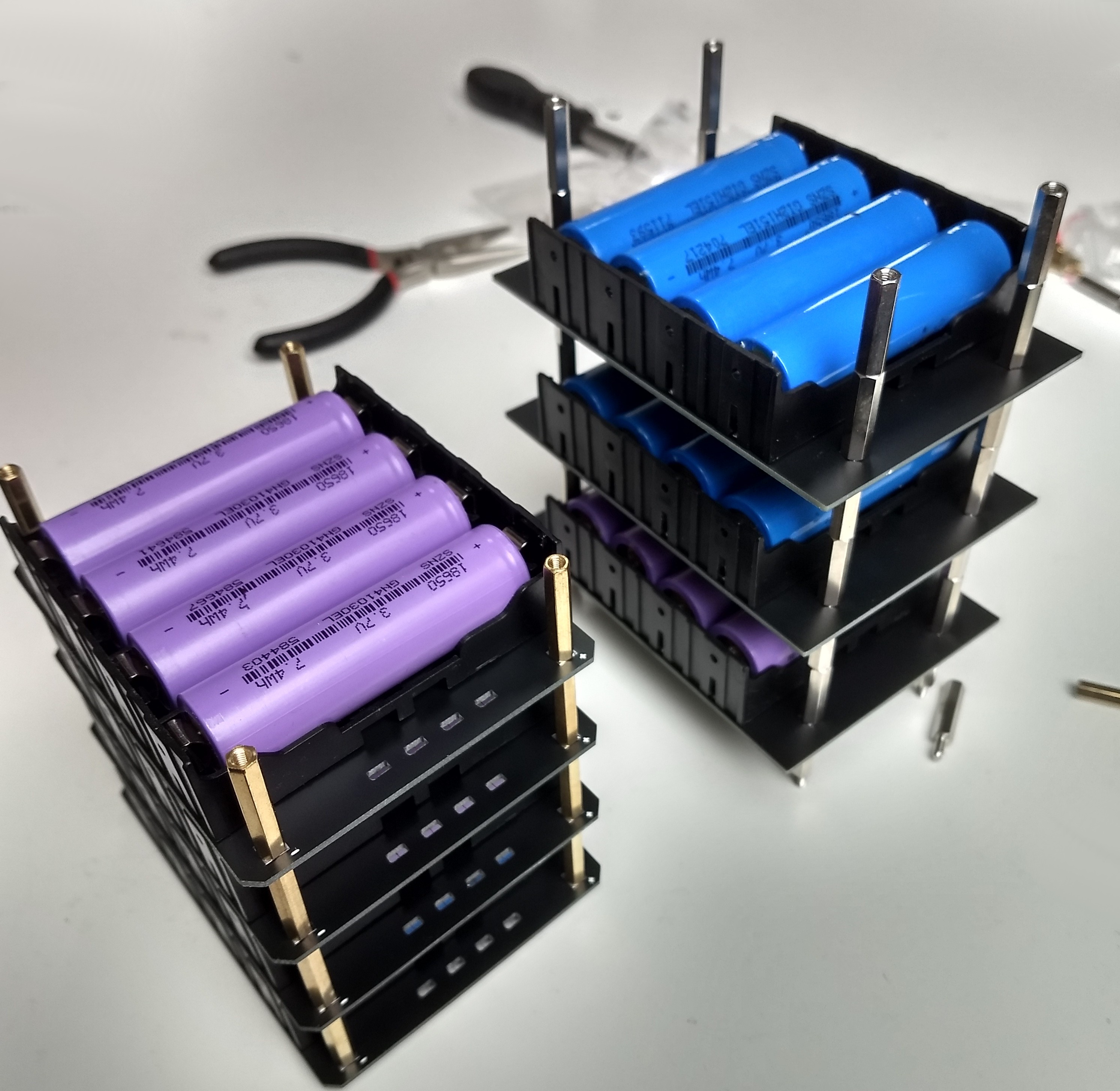
Here is a comparison of v0.3 (left) and v0.2 (right). The general setup is quite similar. Each PCB holds four cells and all PCBs are connected using M3 metal spacers.
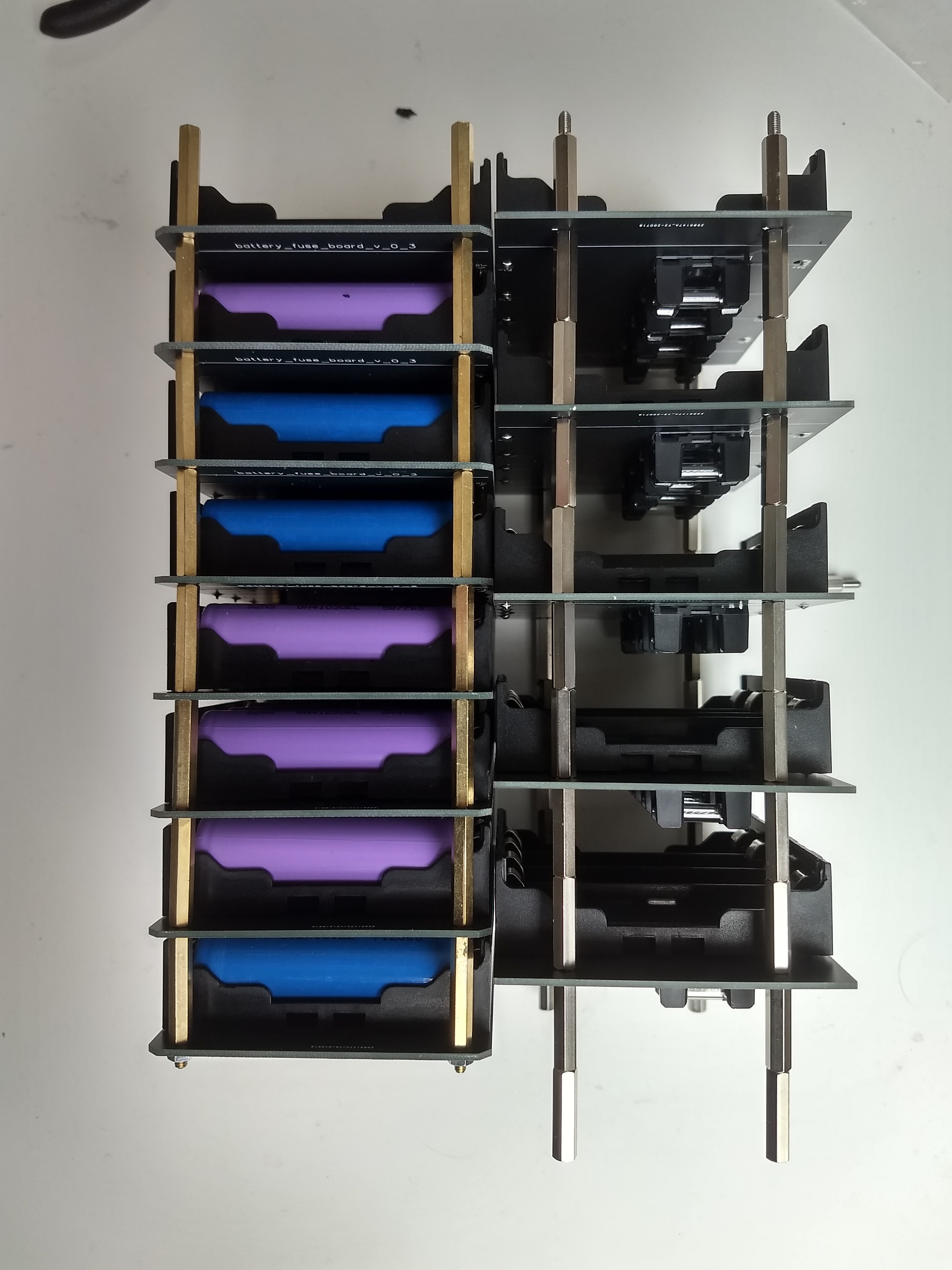
However it becomes interesting when we take a look at the height of the stacked PCBs. As I mentioned in the previous post, I wasted quite a lot of space by using dedicated fuse holders on the backside of the PCBs. With the new PCB version you can see that a lot more PCBs can be stacked with the same height!
Here the final images of the full pack for the powerbank with eight individual PCBs:
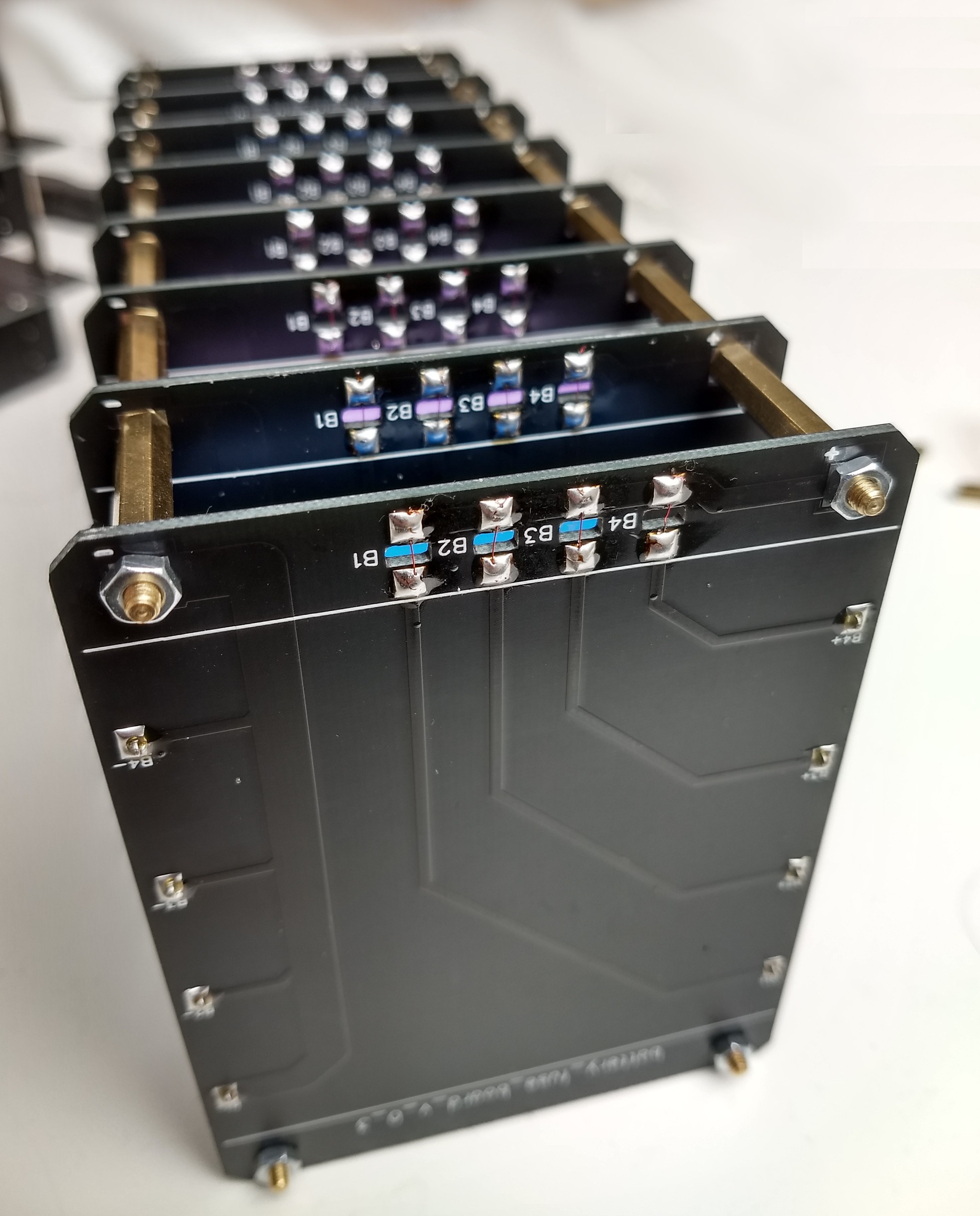
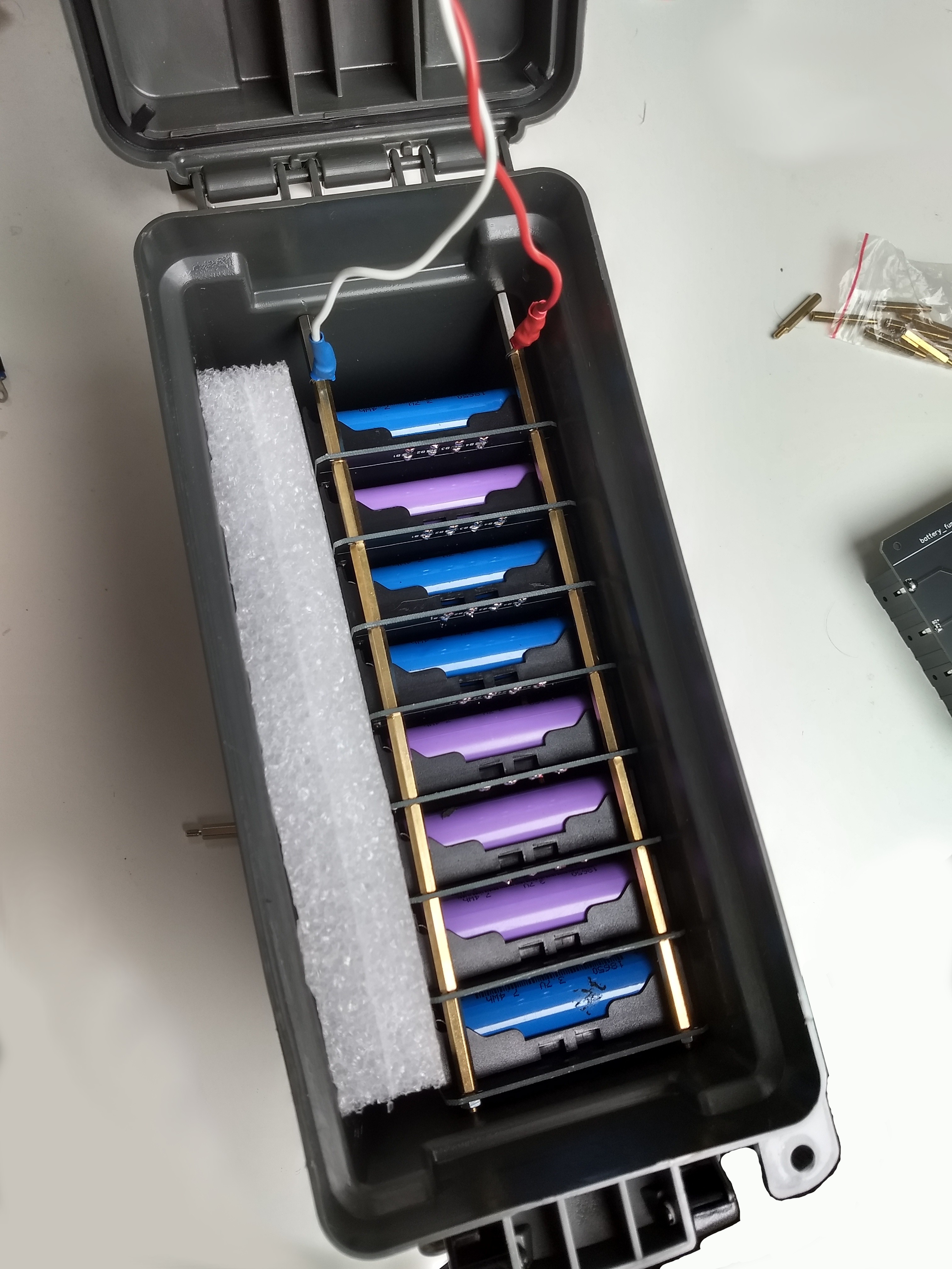
With the height-optimized v0.3 PCB the powerbank has 32 cells in total. The previous PCB only fitted 20 cells in total. This gives around 64Ah of capacity or 236Wh of usable power.
The next steps are to get or design a better charging board which offers more than 18 watts and to build packs with multiple cells in series to get a higher output voltage. But for that the total PCB design has to be changed and will become more complex.
Discussions
Become a Hackaday.io Member
Create an account to leave a comment. Already have an account? Log In.