 Tim
Tim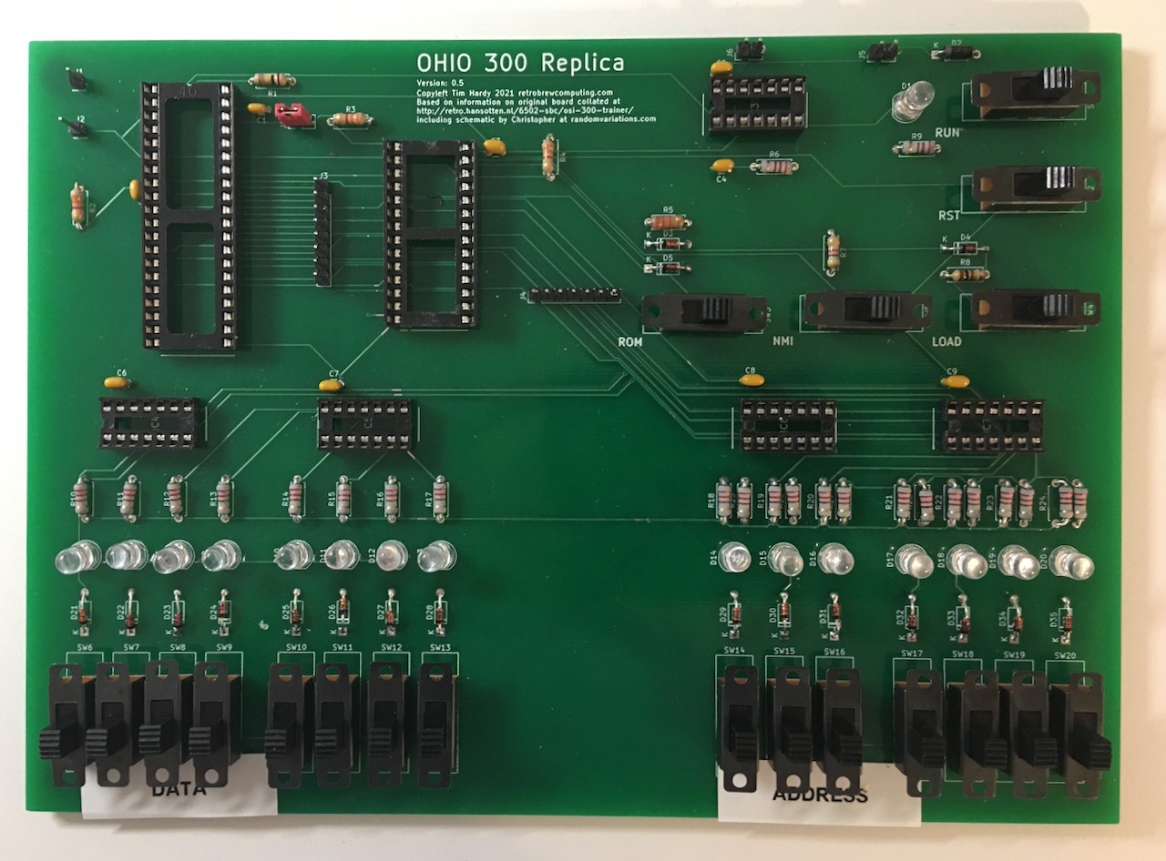
While soldering up the first PCBs which I have optimistically versioned as v0.5 I found a number of errors on the silkscreen - several missing resistor and diode values and, more confusingly, I had managed to swap the DATA and ADDRESS labels. It would also be helpful to label the power pins. The footprints however were fine and everything was easy to solder although the resistors were a little cramped and given how much space this board has I could possibly be a bit more generous here. For a first board though, it's okay.
With 5V powering the board, there's about 4.3V across each IC - except for IC6 and IC7, the SN7417Ns that buffer the address lines and which are connected to ground when the RUN switch is connected to ground. These also have about 4.3V between the VCC and ground pins when the RUN switch is connected to 5V. I expected the values to be closed to 5V and wonder if this might be a problem.
On my replica, the RUN switch is connected to ground when it is to the right. I get the impression from the OSI Manual that in the original this was the other way around so once I have confirmed this is the case I will fix on the next iteration.
With no ICs installed the RUN light stays on all the time.
Once the SN7417Ns and the SN7042N are added, the RUN light stays off. All the data and address LEDs are on when RUN is to the left (connected to VCC). When RUN is switched to the right (connected to ground) the LEDs for data and address can be toggled on or off by the switches.
When the ROM switch is to the left, the data LEDs cannot be changed by the switches. They are not completely off however - there is a very faint glow. I am guessing I need to increase the resistance.
When the LOAD switch is to the left, the data LEDs cannot be changed by the switches.
When RSI is switched left, 5V is asserted on the RESB pin on the CPU.
When NMI is switched left, 5V is asserted on the NMIB pin on the CPU.
So far, so good, more or less.
Adding the CPU and RAM exposes a problem. The data LEDs which I would expect to display random values for each address are mute. It seems unlikely that every value in the RAM is 00000000 - unless I have a dead chip. More likely the read enable logic is not functioning as intended or the RAM is not seeing the address that I am setting with the switches. I didn't however have time to test more closely what was going on at the RAM pins or the CPU.
I noticed some flickering when I physically moved the board and then I saw some data LEDs randomly lighting up which suggests a poor connection somewhere or a short circuit. There were a number of solder splats and some flux residue on the PCB that could potentially cause shorts so I've removed the ICs and given the board a scrub with IPA followed by distilled water. I am going to leave it to dry out thoroughly overnight. I will hopefully find time to continue testing later in the week.
I should probably have touched up the solder joints again before cleaning the board but that can be for another day.
One thing that has become clear to me is that I am not 100% clear in my mind about the expected behaviour of the circuit which of course makes it impossible to test until I have worked this out for myself. This is work I should have done before getting to this point but the whole experience is a learning one and I will remember that for the next time. In truth, I should probably have breadboarded the circuit rather than jump into manufacturing a PCB but I find breadboards intensely frustrating and PCB manufacture is now so quick, cheap and easy that I skipped that step. I hadn't expected this to work flawlessly without any issues and I am fairly confident that I should be able to work out what is going on and fix it. More importantly, I am also having fun!
Discussions
Become a Hackaday.io Member
Create an account to leave a comment. Already have an account? Log In.