 Tim
Tim
Finally had some time to work on this thanks to it being another bank holiday weekend and after some frustration I have got the latest version (0.6) of the board working. Above is the result of the second exercise in the manual.

Toggling in code by hand is hard work and ridiculously easy to get wrong. It is however helping me to develop a more intuitive understanding of lower level coding and is exactly the kind of masochistic pleasure I was hoping for when I embarked on this project!
Those paying close attention may note that the control switches in v 0.6 do not match the historical design. In the next iteration, I will fix this and label their modes explicitly as I have done here temporarily by using a labeller. The Ohio Scientific Model 300 uses the front copper layer of the PCB for the little on-board documentation there is but since we have the luxury of a silk screen it seems worthwhile diverging from the original in this way.
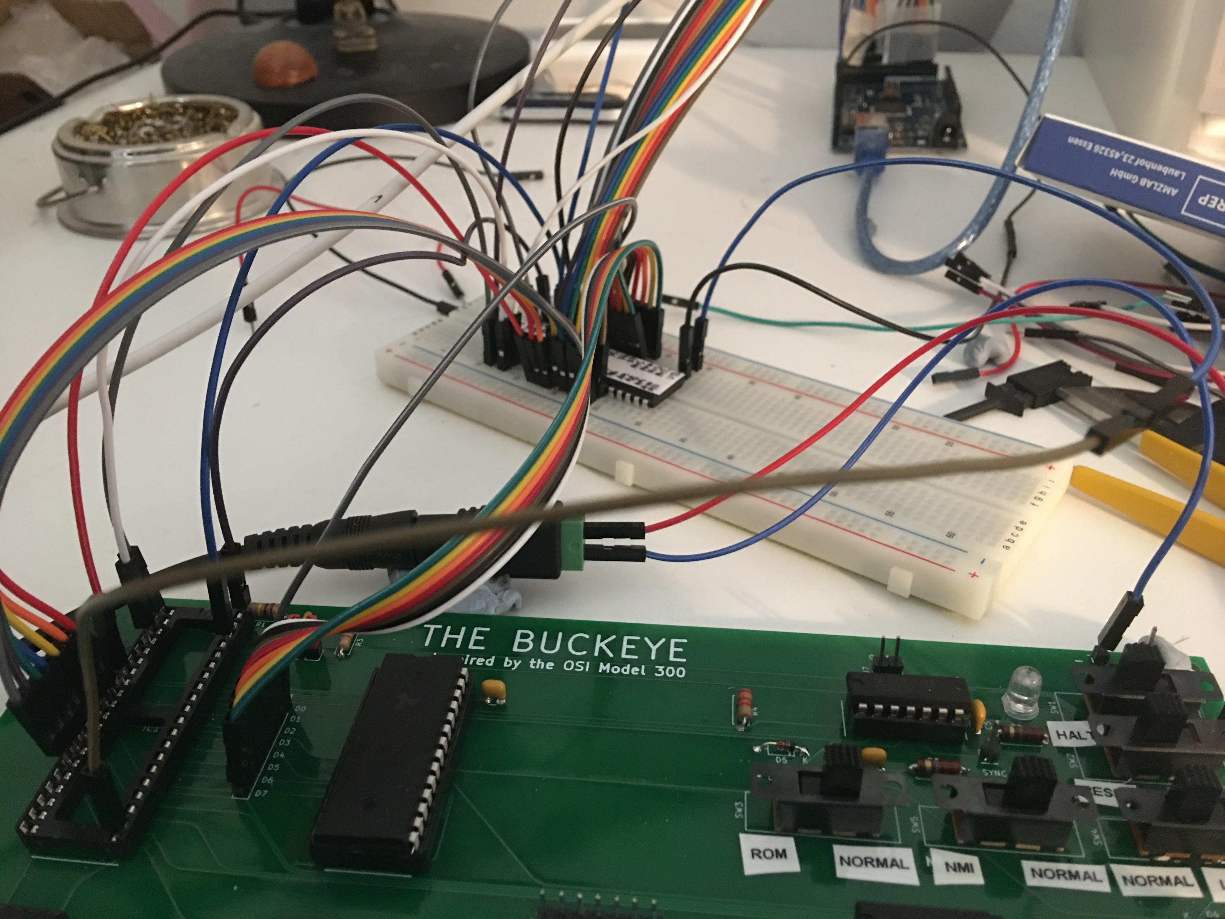
The first version (0.5) of the board was a mess. I had confused the buffered address lines with the address lines leaving so little functioning that it was not even good enough to test. (I could set and read values to one fixed address in RAM and that was it.) This current version (0.6) is much better and I was able to set and read values in RAM without too much of a problem using the switches - once I'd fixed a floating address pin - however I was not able to get the CPU to run any code.
I was not sure where to begin so first I decided to try to work out what exactly was going on as a first step towards working out how to fix it. Inspired by the Ben Eater videos, I ordered a cheap Arduino Mega clone, put the 6502 on a breadboard and used the Arduino to log the changing signals. It became clear that the 6502 was - sometimes - successfully reading the program counter value from the reset vector and was jumping there but was never able to read the value stored at that address.
I was very confused and decided to write some more code to explore this, planning first of all on isolating the 6502 and emulating the RAM so I could confirm that I had not accidentally killed the chip during my various ham fisted experiments. To do so I needed to return to the data sheets to better understand the exact sequence of signals the 6502 expects during a reset and as I studied them it suddenly struck me that the new W65C02S that I am using has a BUS ENABLE (BE) pin which is not present on the old MOS 6502 used in the original design. I had left that unconnected and the fact that it was floating would explain why the CPU could sometimes read the address and data lines and sometimes failed to do so.
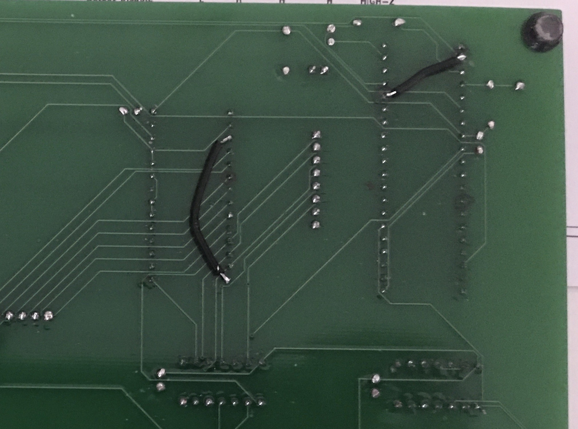
I connected it to the RDY pin with a bodge wire on the back on the PCB and as if by magic the board now works!
(In the photo you can also see that I have also manually tied A7 to ground: I experimented with having an extra switch connected to A7 and when I removed it, I accidentally left the pin floating.)
I'll carry on testing when I get time but I'm pretty confident now that the the next version of the PCB should be the last. I don't think I'll be adding any extra address switches as now that I have experienced the frustrations of doing so I cannot imagine anyone wanting to toggle in more than 128 instructions by hand.
Discussions
Become a Hackaday.io Member
Create an account to leave a comment. Already have an account? Log In.