 Thomas Countz
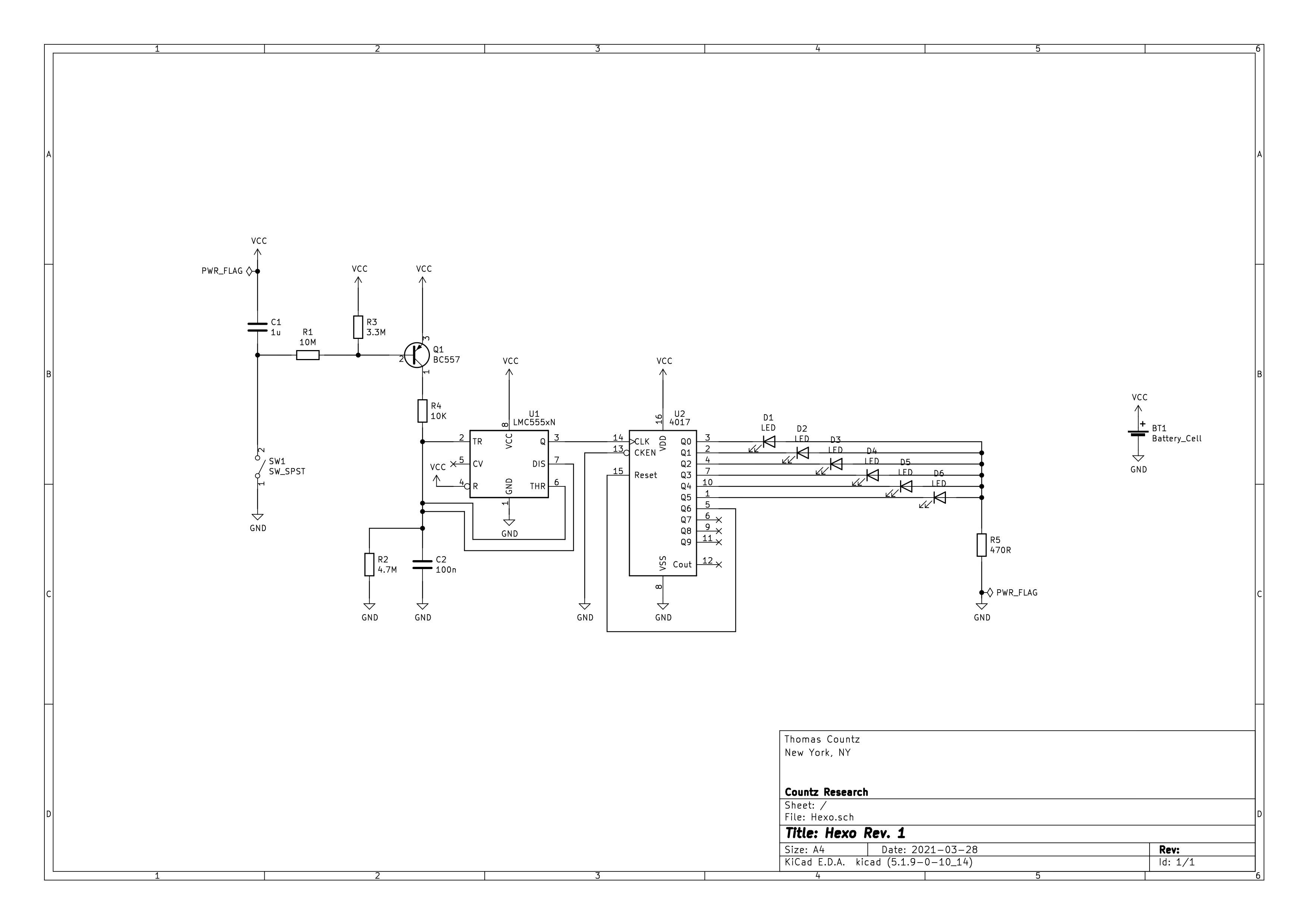 You can find the PDF version of this schematic under the project's documents.
When SW1 is closed, C1 quickly charges to VCC (I think there might need to be a current-limiting resistor between C1 and VCC, though maybe SW1 provides this). After C1 is charged, current begins to flow from VCC through both R3 and the Q1's emitter. Because Q1 base voltage is negative w.r.t. the emitter voltage (Q1 base-emitter voltage), the transistor is active forward and current flow through the collector. (It's a PNP).
Let's continue as if SW1 is still closed. Now that current is flowing through Q1, the 555 begins to oscillate as if it were in astable mode. Charging and discharging C2 to 2/3 and 1/3 VCC respectively and setting pin 3 (output) high and low in kind.
Pins 2 (trigger) and 6 (threshold) are tied together so that the 555 can continue to "retrigger" itself when C2 is discharged and the voltage reaches 1/3 VCC. In a typical astable configuration, a resistor is placed between pin 7 (discharge) and tied-together pins 6 (threshold) and 2 (trigger). This has the effect of adjusting the duty cycle by altering the charging speed of C2. In this circuit, the duty cycle is manipulated by altering the charging speed of C2 by way of a steadily reducing current through Q1 instead.
(Note: I believe there should be a decoupling capacitor at pin 5 (control voltage)).
Now that the 555 is oscillating, pin 3 (output) sends a square wave clock pulse to the 4017 pin 14 (clock). The 4017 is a decade timer and at each rising edge of the clock pulse it will consecutively set each of it's 10 output pins high. Only one pin is high at a time, the other are low. In the case of this circuit, we're only interested in using 6 of the 10 outputs, so we tie pin 5 (Q6), the seventh pin to be set high, to reset which will cause the 4017 to set it's first output (Q0) high instead.
All of these outputs are used to drive LEDs which whose cathodes are connected to a common current limiting resistor before being tied to ground. These LEDs will continue to be turned on and off consecutively as long as a clock pulse continues to drive pin 14 (clock).
Let's continue now as if SW1 is opened after being closed. Once SW1 is open, C1 begins to discharge and current continues to flow through VCC and GND by way of Q1. As C1 discharges, however, Q1 base-emitter voltage begins to climb, i.e. the base voltage starts to become less negative w.r.t. the emitter voltage. As this is happening, less current is flowing through Q1 and C2 is taking longer and longer to charge and therefore the clock pulses from pin 3 (output) of the 555 are beginning to slow (the time between clock pulses is increasing). This has the effect of diminishing the speed at which the 4017 is cycling through the LEDs.
Eventually, Q1's base-emitter voltage reaches the cutoff threshold (~-0.6v) and current stops flowing through Q1. C1 continues to discharge, however, through R3. At this point, whichever LED the 4017 had set to high last, remains lit.
I'll include a simulation in the next update so that you can see all of this in action with either LTspice or Falstad.
Discussions
Become a Hackaday.io Member
Create an account to leave a comment. Already have an account? Log In.