 Joel Kozikowski
I finally got a chance to run some etch tests with the new unit, and sadly it failed. Exposure time went from about four minutes up to 8+ minutes, and the results were almost unusable. As predicted in the project discussions, there was a lot of defocus problems around the edges.
I have ordered three different UV sources to try as alternatives: one is a different LED strip with a higher concentration of LEDs and is intended to use for UV curing, and two are the actual UV sub-systems from two different mSLA printer manufacturers.
To create a baseline (and to prove that this was only a minor setback), I went back to my prototype and made a few minor adjustments based on community feedback: Using the original "UV floodlight" I was using in the prototype, I increased the distance from the LED panel to the LCD by about 3 inches. I also centered the LEDs around the copper board (to remove the "uneven exposure" I had originally dealt with). Doing these changes, I got the best exposure and etch I've had so far, so this is my new benchmark.
Here is the sample "circuit" I used for testing:
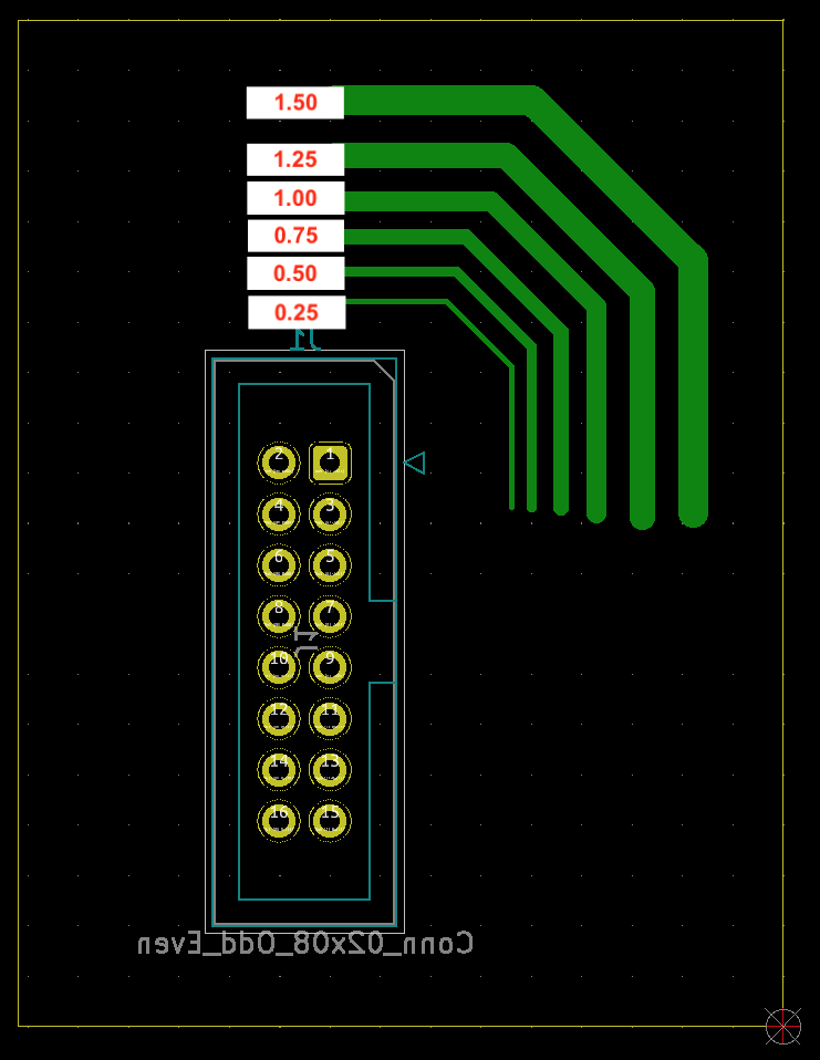
Notice I am testing for traces between 0.25 mm and 1.5 mm.
Here is what the board looked like after a 4 minute and 30 second exposure, then 2 minutes and 15 seconds in a "developer" mixture consisting of 10 ounces of water and 3/4 teaspoon of 100% lye drain opener:
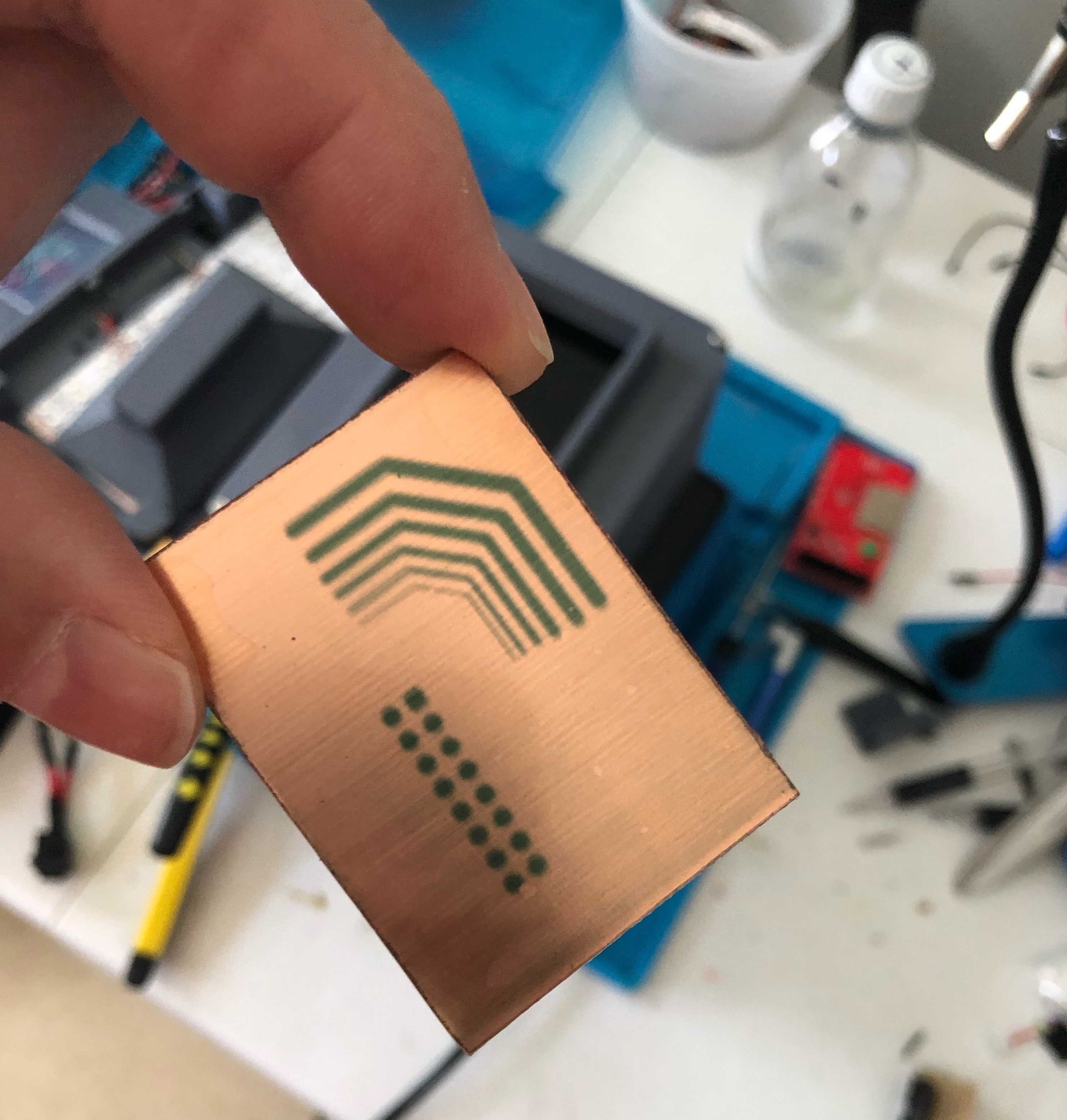
I then put the board in a small container of ferric chloride for 43 minutes, and this was the final result:
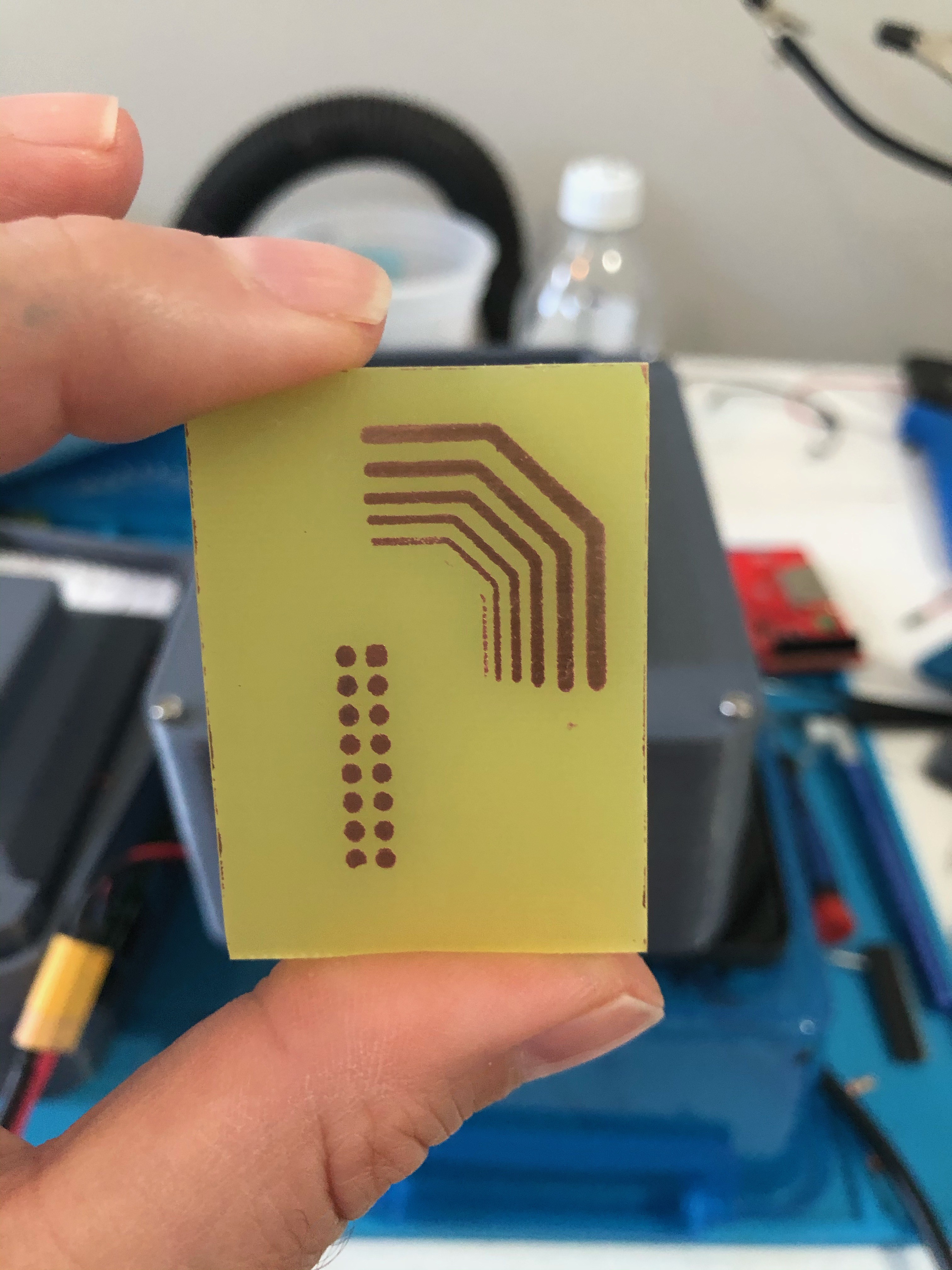
You can see that the 0.25 mm trace was over etched a bit, the 0.5 mm trace is mostly in tact, and the 0.75 mm and beyond traces are perfect. All but one of the 16 pads for the IDC16 connector came out well, and it's fairly easy to see the difference between the square pad of pin #1 and the and round pads of the other pins.
I'm pretty happy with these results. It is more than useable for prototype boards, which is what this device is intended for.
During the etching process, I had time think about things and already plan for the future. For sure I am going to ditch the ferric chloride (first time I've tried it) and go back to the muriatic acid and peroxide mix that I've used before. Ferric chloride is way too messy, but more important: you can't see the board as it's etching to see when it's done. The 0.25mm trace may very well have survived if I had pulled it out just a little earlier. It seemed in tact the two to three minutes prior when I did a spot check.
Another huge idea: I've been thinking about a way to make it quick and easy to apply a solder mask to the board. Solder masks are applied and cured pretty much the same way that the 3d printing resin was applied on the YouTube hack video that inspired this project. If I can come up with a quick way to evenly and consistently apply liquid resin while eliminating mess, this device should handle resin as a much better etch resist, which would eliminate the "developer" step. Also - the exact same process would apply to solder mask.
Discussions
Become a Hackaday.io Member
Create an account to leave a comment. Already have an account? Log In.