 Joe Wingbermuehle
Following up on my search for faster transistors, I got the boards back earlier this week to test a new candidate transistor (a 2SK3018 vs 2N7002). The good news is that the surface mount switch I wanted to try appears to work just fine. Unfortunately, the new transistor does not appear to improve performance nearly as much as I had hoped.
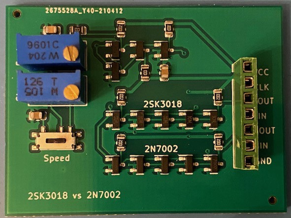
For the test, I have the output of an oscillator tied to an inverter implemented with 4 transistors of each type in parallel (I ended up going with a NOR structure instead of a NAND structure). The graph below shows the results.
The blue line is the output fo the 2SK3018 inverter and the yellow line is the output of the 2N7002 inverter. There is maybe some difference, but it's hard to see here.
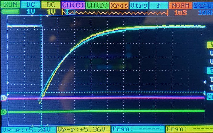
To investigate further, here is the input compared to the output for the 2N7002 inverter:
The output is in yellow and the input is in blue. The threshold voltage is apparent and seems to be around 1.6V. After somewhere around 1.8us, the input has reached 2V.
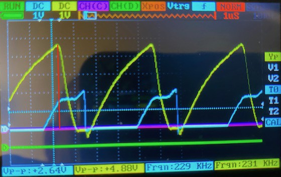
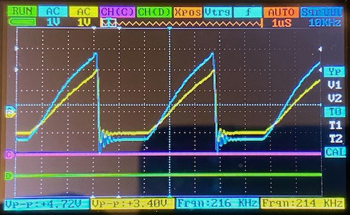
Nothing too surprising. Here's the 2SK3018:
Again, the output is in yellow and the input is in blue. Here we see a lower threshold voltage of what appears to be 1.2V. Unfortunately, after 1.8us, the input has only reached 2V. This is actually quite similar to the 2N7002.
Looking at the data sheets, although sparse on details, maybe this isn't completely unexpected. For the 2N7002, the maximum capacitance is given as 50pF and no typical capacitance is listed. For the 2SK3018, only a typical capacitance is given as 13pF.
The lower threshold is an advantage, but we need to make sure that external components that the Q2 uses, such as the SRAM and LCD, still get a high enough voltage for the high level. In the end, I'll probably just go with the cheapest transistor for the next revision. Although it would be nice to get some more speed, I would like to be able to do so without adding significantly to the size or power requirements of the Q2.
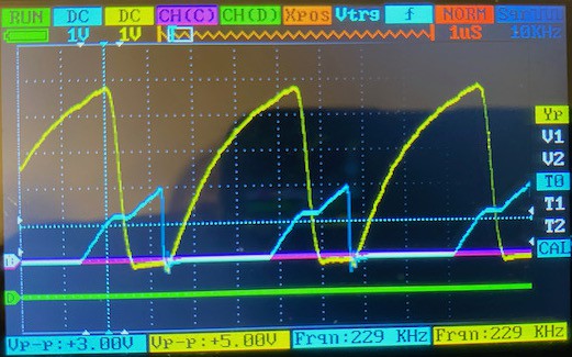
One, perhaps obvious, observation from this experiment that might speed things up is that in NMOS gates with a lot of inputs are slow. The graph below compares two 4-input NAND gates. For the NAND gate in yellow, the first input is switched (closest to ground). For the NAND gate in blue, the last input is switched (other inputs are held high).
When the first input is switched the output only reaches 3V after 2.4us whereas when the last output is switched the output reaches 4V. I'm guessing this effect is due to the output capacitance combined with the on-state resistance. For the address decoder, there is a 12-input NAND gate to check for 0xFFF, which is very slow and probably limiting performance. I plan to revisit that with a more appropriate pull-up. This also implies that re-arranging the order of signals into the gate may improve the speed of the gate (slower signals should go near the output side, and faster signals near the ground side). NOR gates don't slow down with increased inputs quite as much as NAND gates, but still slow down as the number of inputs increases almost certainly due to the output capacitance.
Discussions
Become a Hackaday.io Member
Create an account to leave a comment. Already have an account? Log In.