Andy Birch
Introduction
Most electronic systems can be explained using this diagram.
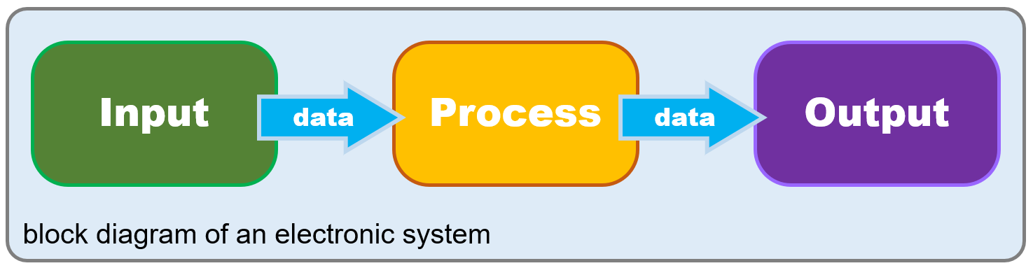
Systems consist of inputs that connect to the outside world, some form of processing or control and outputs to interact with the outside world.
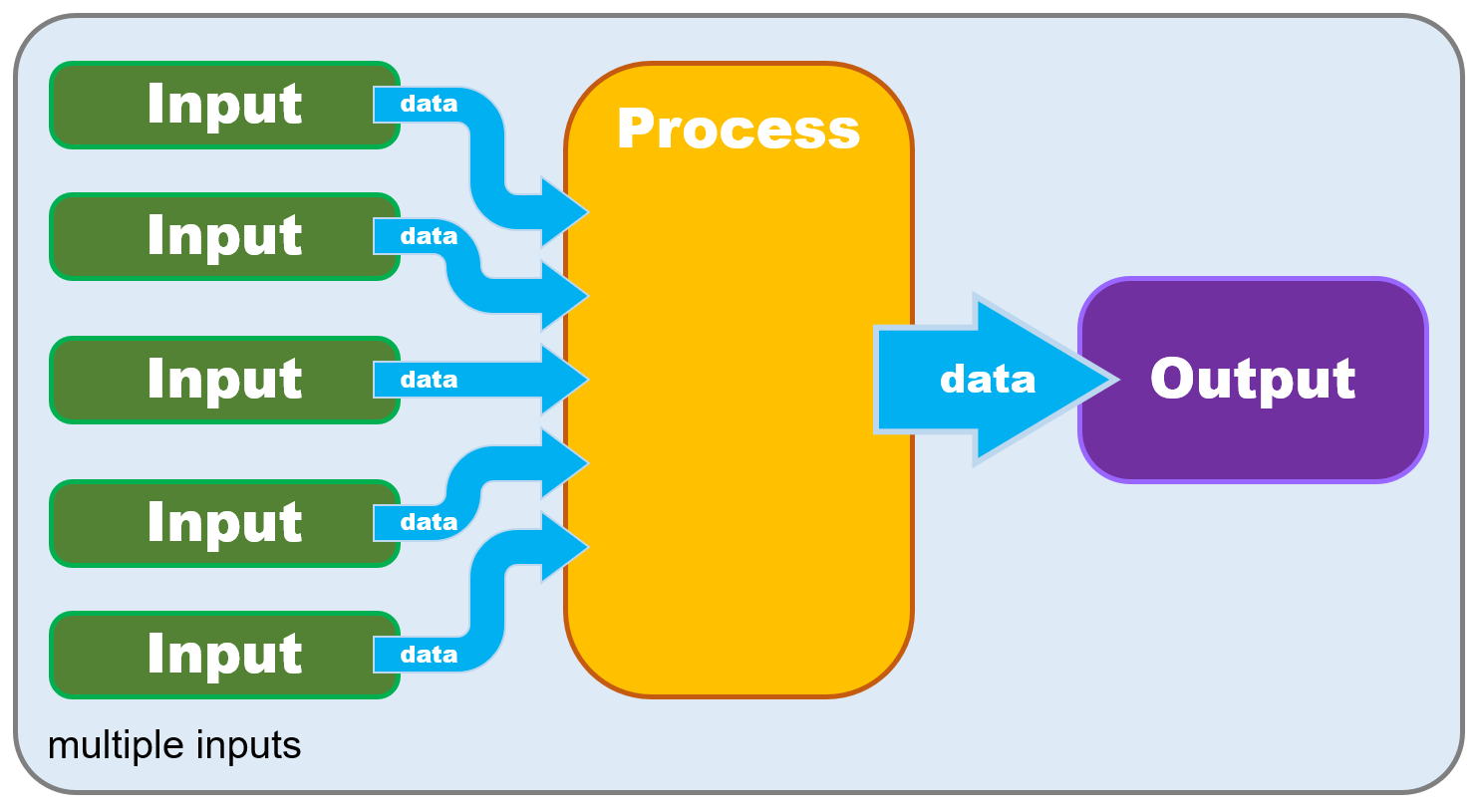
If the system needs multiple inputs (buttons, potentiometers, sensors), you either run out of pins to connect to or you expand your circuit, making it more complex.
Not Enough Pins
As with most microcontroller projects you can quickly run out of pins. Especially analog inputs. A common technique to solve this is to use a multiplexer/demultiplexer. There are analog and digital versions. A common chip that is used is the 4051.
The following is from the Texas Instruments Data Sheet - CD405xB CMOS Single 8-Channel Analog Multiplexer/Demultiplexer with Logic-Level Conversion
“The CD4051B, CD4052B, and CD4053B analog multiplexers are digitally-controlled analog switches having low ON impedance and very low OFF leakage current.”
“The CD4051B device is a single 8-channel multiplexer having three binary control inputs, A, B, and C, and an inhibit input. The three binary signals select 1 of 8 channels to be turned on and connect one of the 8 inputs to the output.”
 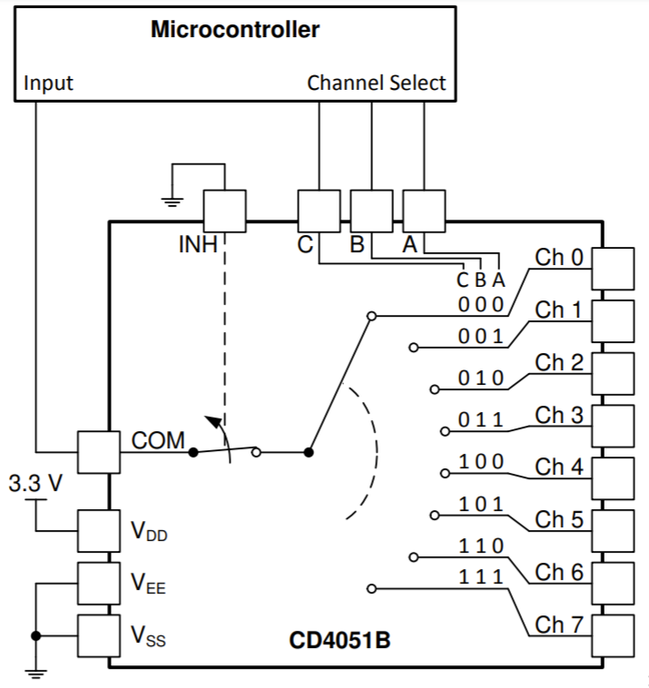 NOTE In this example the 4051 is being used to connect multiple inputs to one pin but the 4051 will work in either direction. |
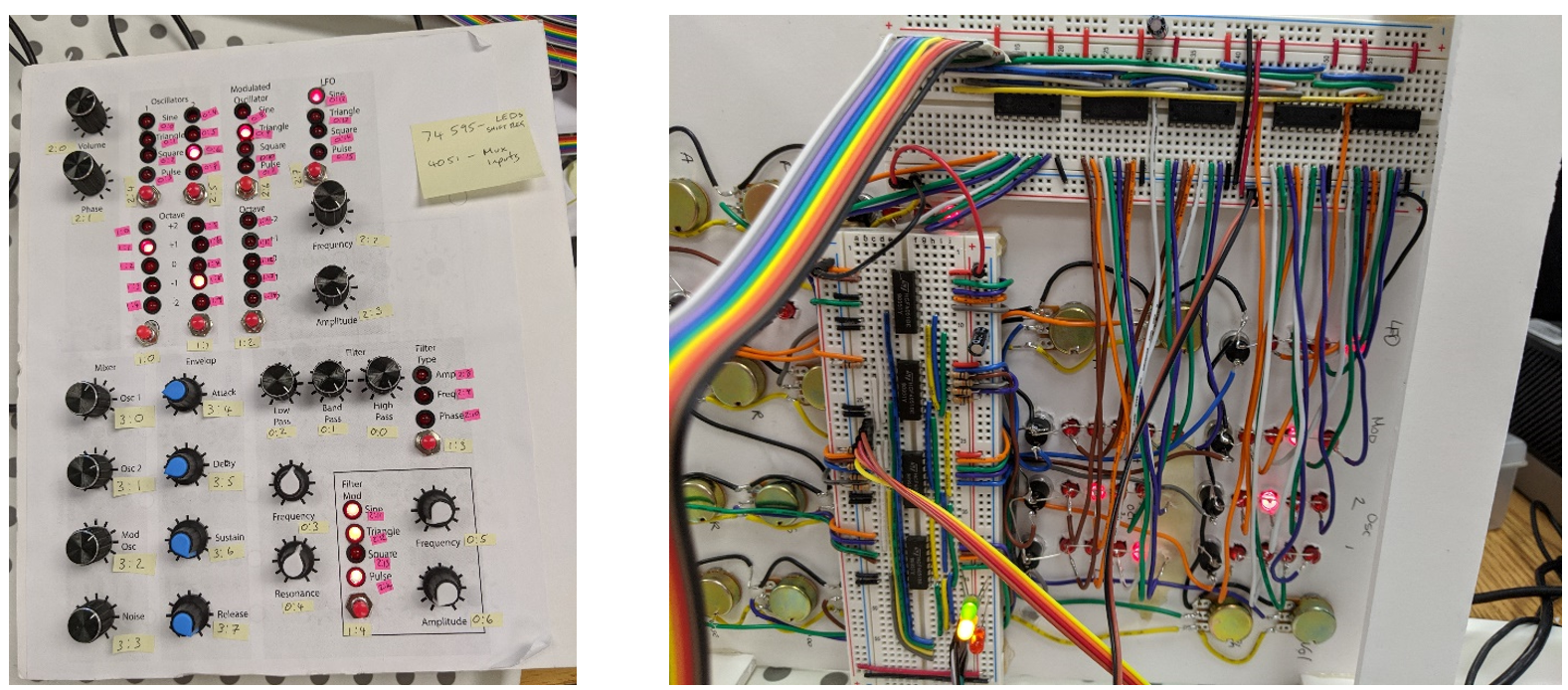
Although I have used 4051 MUX in previous projects, I found that similar problems would occur with each new system I created. I would lose track of what pin on the 4051 mux was connected to the pins on the microcontroller. Each mux needed a set of control pins (C, B, A) and analog input, so I would quickly run out of pins. Plus, I had to totally rebuild the circuit each time I wanted to try something new.
Here is my example synth project again. It worked ok but when I started to work on it again after a few weeks break I struggled to continue with its development due to the circuit’s complexity.
Initial Idea
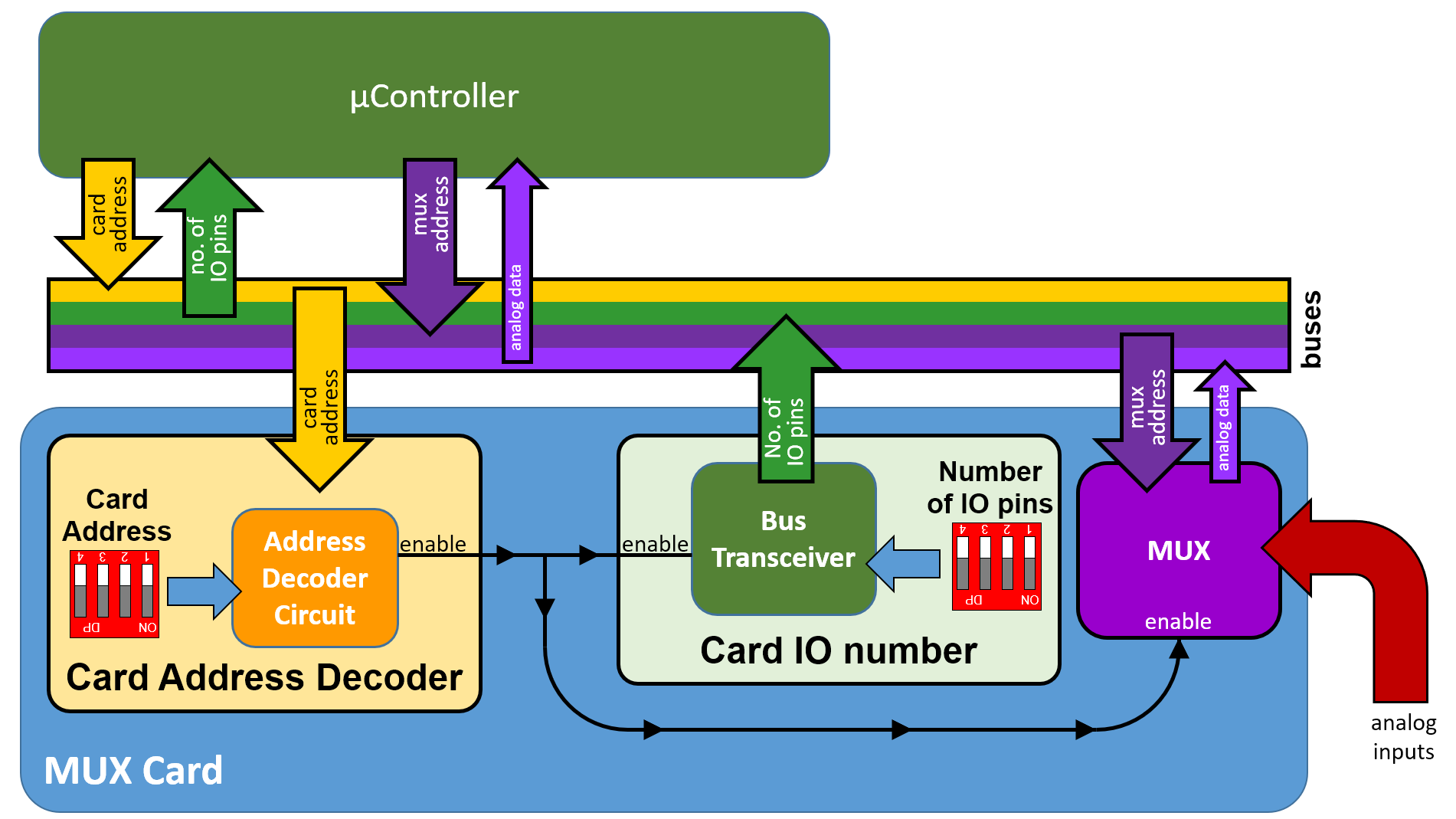
I had the idea of designing a system that would allow me to add as many MUX circuits as needed without the need to modify the code too much. I could use a bus to carry the signals to and from each MUX card circuit.
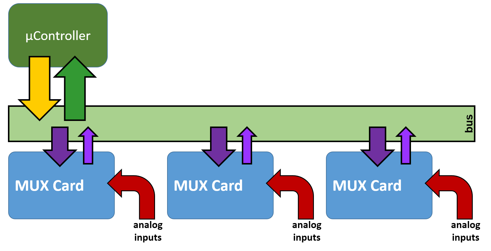
The microcontroller connects to each card via the bus(es)
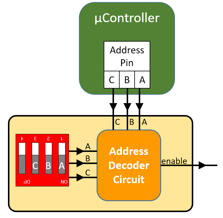
My idea was to make each card have a unique address that the microcontroller could use to enable each card independently.
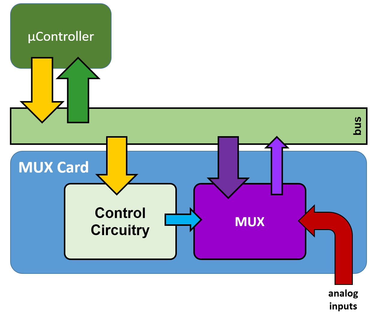
Each card would require control circuitry to read the address from the microcontroller and enable that cards MUX.
Control Circuitry
Initially I planned to use just three address lines from the microcontroller. This would give me 8 possible addresses for the MUX cards. Each MUX can have 8 inputs so 8 cards x 8 inputs = 64 possible inputs.
| NOTE: The system is designed to allow me to add another address line later if needed. 4 address lines = 16 addresses. 16 cards x 8 inputs = 128 inputs. Also if needed it is possible to put multiple MUX chips at each address giving more inputs or you could use a 16 channel MUX. e.g. a 74HC4067. |
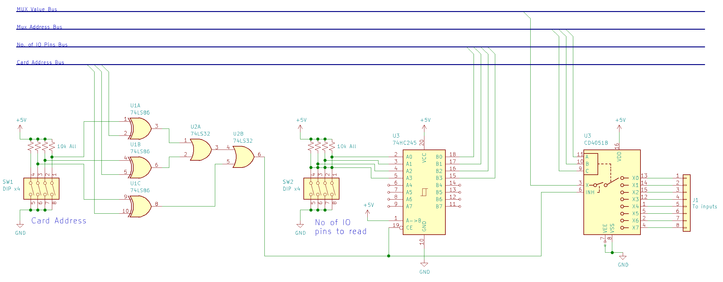
The MUX card needs to control the enable pin of the MUX. To do this it reads the address from the microcontroller. If the address is identical to the cards address, then enable the MUX. If not, then disable the MUX.
The 4051 MUX control pin is called INH (pin 6). A high signal disables the MUX. Therefore, the control circuit needs an output that goes low when the correct address is read.
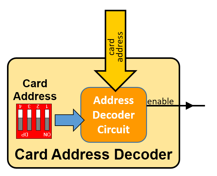
Here is a block diagram of the address decoder.
I will use a DIP switch x 4 to set the address of the card.
| NOTE The switch is shown upside down as I plan to use pull up resistors. |
Designing the Control Circuitry
The enable needs to go low when:
microcontroller address pin A = DIP Switch A
microcontroller address pin B = DIP Switch B
microcontroller address pin C = DIP Switch C
There are several techniques to design a logic system to do this but…
Looking at an exclusive OR gate you can see that when its two inputs are the same you get a logic 0.
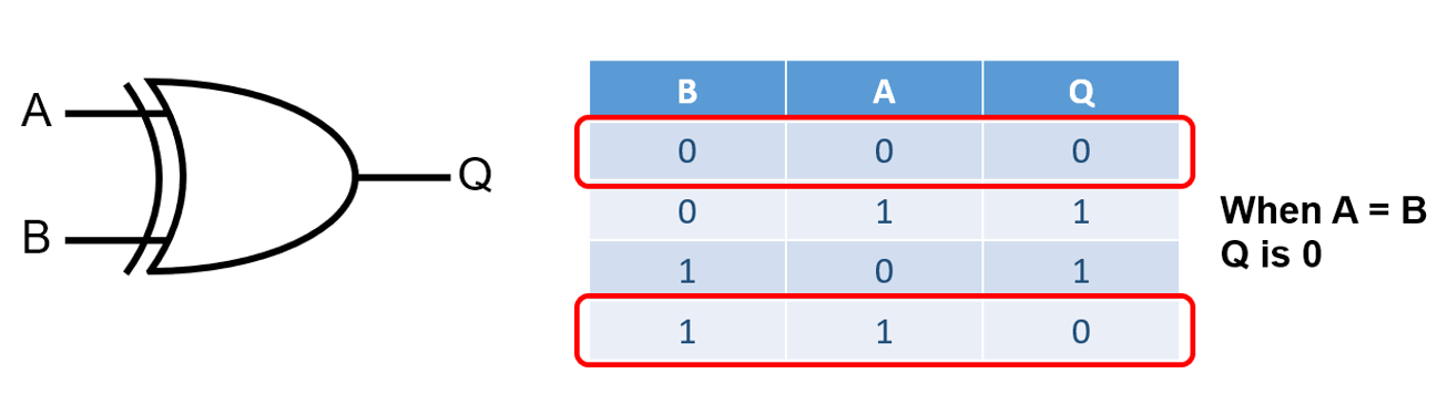
Therefore, each address line from the microcontroller and each line from the DIP switch need to be XOR’d.

These then need to be combined in a way that will pass the 0 or 1 to the output.
OR gates will do this – the only way to get a zero is if all outputs from the XORs are zero.
This circuit will give a low enable when the address from the microcontroller is the same as the DIP switch.
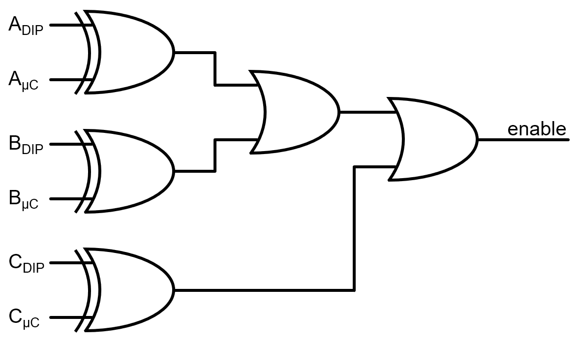
Here is the full circuit for the address decoder and the MUX.

Number of Inputs
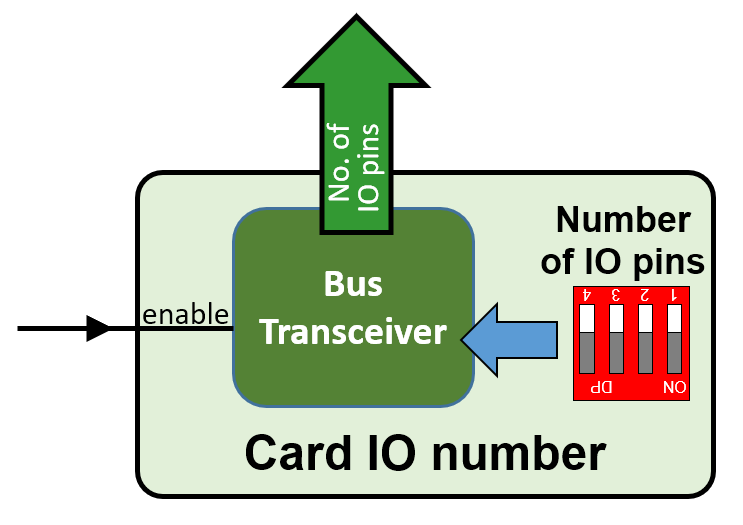
At this point I realised that I may not want to use all 8 inputs on every MUX. Any unused inputs being checked by the microcontroller will slow down the system.
I added another DIP switch and a bus transceiver to each card. The second DIP switch allows the card to send the number of IO pins to read to the microcontroller. A bus transceiver is used so that each card will only send the value when that card is selected. (plus, these were the chips I had)
Here is the block diagram.
Here is the full block diagram for a single card.
Bus Transceiver
I used a 74HC245 Octal Bus Transceiver to link to the bus.

The enable (CE) pin also needs a low signal so I can use the same signal as the MUX enable.
The only other connection on the transceiver is a direction pin, set to 5v for the direction I used – A to B.
Again, I used pull-up resistors on the DIP switch.
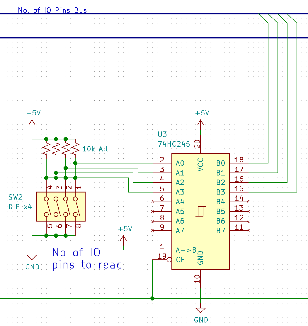
When the enable (CE) is pulled low the transceiver connects its input (A0 – A7) pins to its output pins (B0 – B7).
When enable (CE) is high the output pins are not connected to anything.
Complete Circuit Diagram