 Enki
EnkiDNS-320L NAS
Table of Contents
- 1. Intro
- 2. Hardware
- 3. Bootloader
- 4. Original firmware
- 5. Building mainline Linux kernel
- 6. Building a rootfs
- 7. Bootloader setup
- 8. References
1 Intro
The D-Link DNS-320L is a simple 2-bay SATA NAS device which can run multiple versions of Linux. This post provides information on how to run the newest (at the point of writing) mainline kernel on it without patching as well as how to build a simple initramfs using buildroot. This is a bit different than other projects building Linux which usually focus on using debian packages.
2 Hardware
There exist at least four versions of the hardware, I own two of them and the ones that I own can be distinguished by using the following features:
| Version | P/N on bottom label | HW version on bottom label | U-Boot banner | Other distinguishing marks | Notes |
|---|---|---|---|---|---|
| DNS-320L A1 | Referenced here | ||||
| DNS-320L A2 | Referenced here | ||||
| DNS-320L A3 | ENS320LM…..A3E | H/W Ver.: A3 | U-Boot 1.1.4 (Aug 22 2012 - 17:06:54) Marvell version: 3.6.0.DNS-320L.01 | Text "TWO BAY NETWORK ATTACHED STORAGE" on top plastic cover | Only 100 Mbit link working? |
| DNS-320L A4 | ENS320LM…..A4E | H/W Ver.: A4 | U-Boot 1.1.4 (Apr 17 2014 - 17:31:34) Marvell version: 3.6.0.DNS-320L.01 |
In the A3 version I have only the 100 Mbit Ethernet link is working contrary to the NAS being advertised as supporting 1000 Mbps Ethernet. This is broken both in the stock firmware and in the kernel that I have built so I suspect it's some hardware problem. Is this a bug on this board revision or is my particular NAS damaged I do not know.
There are differences between the A3 and A4 versions in the type of memory chips and used Ethernet transformer. Other than that I have not noticed any differences.
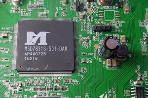
The system is based on a Marvell Kirkwood 1GHz SOC, other chips include an Ethernet controller, flash, RAM as well as an MCU which is a systems management controller similar to what you would have in a laptop or PC. The NAS has it's page on both deviwiki and new wikidevi where detailed information about the chips on the board can be found. The main board looks like this:
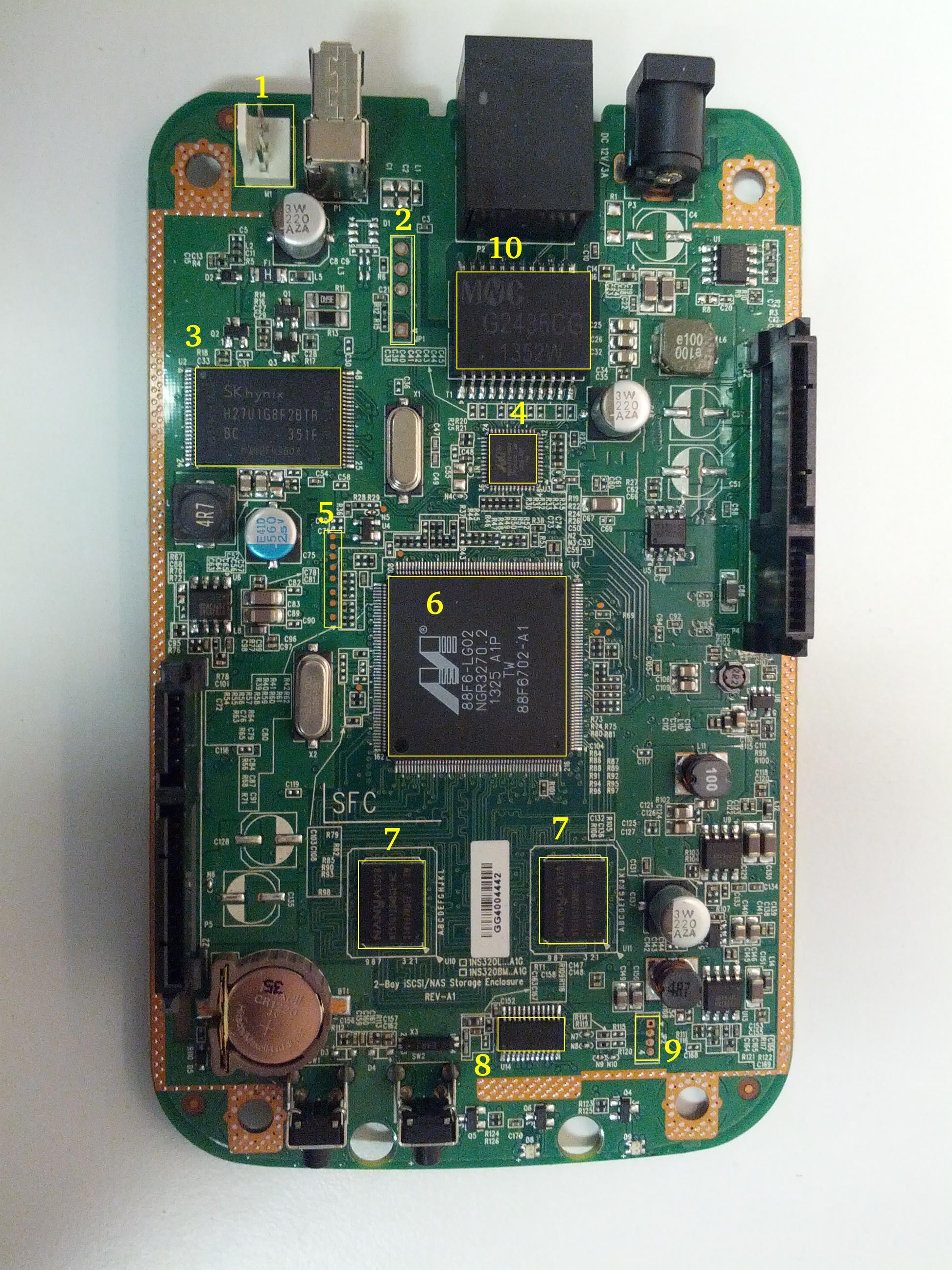
| Number | Label | Chip type on A3 board | Chip type on A4 board | Description |
|---|---|---|---|---|
| 1 | M1 | Fan: AVC DS04010B12U | The fan connector | |
| 2 | JP1 | The serial console | ||
| 3 | U2 | Hynix H27U1G8F2BTR | NAND flash | |
| 4 | U3 | Marvell 88E1318R | Ethernet chip | |
| 5 | Testpads (likely JTAG) | |||
| 6 | U7 | Marvell 88F6702 | The CPU | |
| 7 | U10,U11 | Nanya NT5TU128M8GE-AC | Hynix H5PS1G83KFR | RAM chips |
| 8 | U14 | Weltrend WT69P3 | The system management MCU | |
| 9 | JP2 | WT69P3 programming bus? | ||
| 10 | T1 | MNC G2436CG | MNC G2497CG | Ethernet transformer (datasheet) |
In order to access the unpopulated pads on the board I soldered two pin connectors, because the JP2 pitch was smaller than the standard 2.54mm pinheads I had I used some wire to route it to where it can be accessed:

The board contains four LEDs with the following purpose:
| Label | Color | Description |
|---|---|---|
| D6 | Blue | Power-on and booting indicator LED |
| D7 | Red | "USB" LED |
| D8 | Red | SATA1 port activity LED |
| D9 | Red | SATA2 port activity LED |
2.0.1 Weltrend WT69P3
The WT69P3 is a systems management MCU which controls the power to the board, provides an RTC for time keeping and controls the fan. The MCU is connected via a RS232 link with the main CPU and in the original firmare a daemon in the system communicates with it. The communications protocol has been reverse-engineered and there exist at least two independent open-source implementations of the manamgement daemon - https://www.aboehler.at/hg/dns320l-daemon and https://github.com/martignlo/DNS-320L.
2.0.2 JP2 connector
This connector seems to terminate an I2C bus. Both lines have pullups to +3.3 V and the Weltrend chip's ISP protocol is I2C according...
Read more »

 Machinehum (Ryan Walker)
 Reimu NotMoe
I suppose you need to buy it on ebay, I bought it used as well. As to whether all of this would work on more current units this depends on multiple factors:
- whether you can build a firmware yourself, this requires the Linux kernel to support the CPU as well as all of the drivers you care about (for example SATA), you might have to search for GPL code releases, device trees (like I did) or other stuff
- whether you will be able to boot your fw either by accessing the bootloader (like I did), using the builtin fw update procedure or something else