 Bud Bennett
There seems to be a need for stand-alone step-up and step-down DC/DC converters in Radio Controlled aircraft. I'm thinking about possibly making a long range quad copter that runs on a single Li-Ion 18650 battery. Unfortunately, most FPV cameras and video transmitters can't operate much below 5VDC or 3.3VDC, whereas the battery can drop to 2.5V before it is exhausted.
Step Down (Buck) Converter:
I was watching a YouTube video where a guy was using a step down converter to power a GPS unit separately from the flight controller power supply of a quad copter in order to acquire satellites faster and get a lock. He uses an iFlight Micro BEC to step down the battery voltage (8-25V) to the 5VDC required to power the GPS. (BTW: the GPS only draws about 50mA @ 5VDC.) The Micro BEC dimensions are 14mm x 11mm x 1mm, and it weighs 0.8g. It's not cheap.
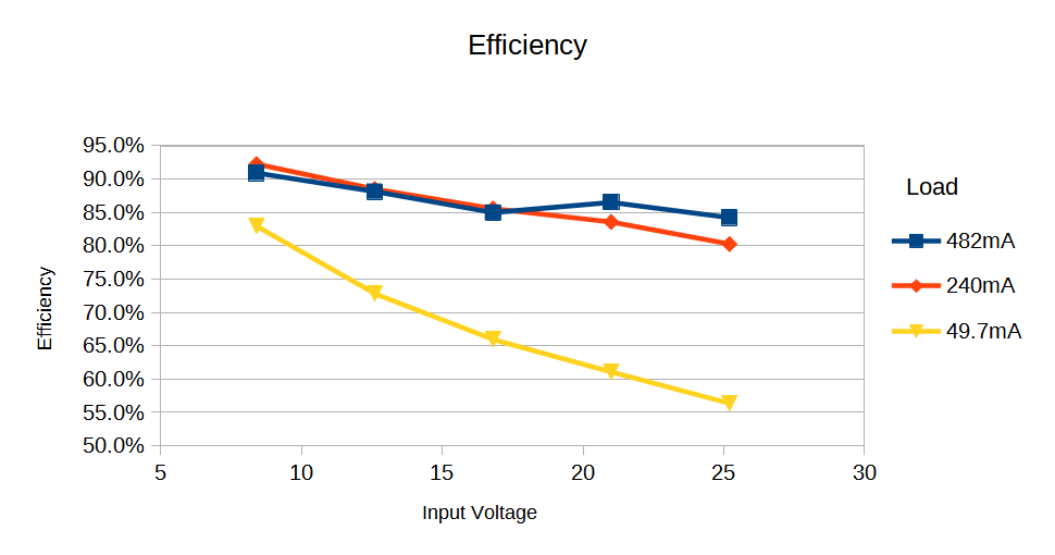
I went to AliExpress to see what was available in the same category and purchased a lot of 5 3A DC/DC step down converters for $0.28, with $6 shipping from the U.S. These units have dimensions of 17mm x 11mm x 4mm. It weighs about 1.5g without wires. They arrived pretty quickly and I verified their functionality and parametrics. I replaced the potentiometer on one unit with a 36k resistor to get 4.97VDC output. The unit has an overtemperature shutdown that kicks in around 1.8A -- it shuts off the output, cools down, and turns the output back on. A practical upper limit of continuous current is probably around 1.5A, with short bursts above that. I did take some efficiency data at one load current point:
I also designed my own buck converter, just to see what was involved and if I could make something smaller and lighter.
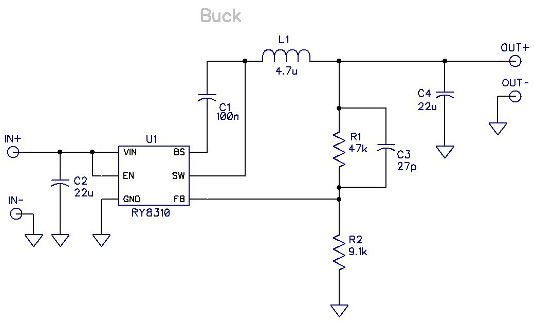
All of the components came from my current inventory: 0805 caps, 0603 resistors, 2x1.6mm inductor, and the RY8310 is a SOT23-6 package. The Rychip RY8310 is a 1.4MHz synchronous buck, with input voltage limits of 4-30V and 1.5A peak current output . The inductor is a VLS201612HBX-4R7M-1, rated at 1.1A (ITemp) and 1.2A (Isat).
I was able to pack the components onto a 14mm x 8mm PCB, which I ordered in 2oz. copper from OSH Park. When the board arrived I found out that I did not have a 22uF 0805 cap with a voltage rating above 16V, so I used a 1210 cap instead.
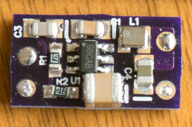
It fit...just barely. Weighed in at 0.48g. Not bad.
I tested just a few parameters so far. Output voltage = 4.97V, over a 7V - 25V input range. It will put out 650mA continuously (with no measurable voltage drop), but gets too hot and shuts down with a 1.3A load.
The output ripple voltage is about 20mVp-p (no load), and pretty clean.
I took some efficiency measurements at a few load currents:
Sidebar: Switched-mode converter vs. Linear Regulator Efficiency
You might look at the chart above and think "Why is he doing this for a lousy 56% efficiency? I'm just gonna use a linear regulator." Well let's examine that thought.
For the "poor" efficiency case above the converter was outputting 250mW, and was requiring 450mW input power. That's a loss of 200mW. An ideal linear regulator would consume 1.26W, with a loss of 1.01W. That still doesn't seem so bad until you consider the temperature rise that 1W of power would produce on these tiny PCBs.
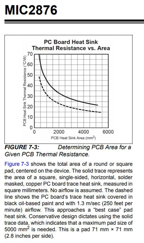
My fat finger estimates that the thermal resistance of a 10mm x 10mm PCB in free air would be around 100C/W (maybe more). Here's a plot of thermal resistance vs. PCB area from the MIC2876 datasheet. To add insult to injury, the converter will probably be covered with heat shrink tubing.
The buck converter temperature rise would be around 20C, where the linear regulator would cook at 100C. I can leave my finger on the buck regulator without getting burned (<50C), but I'd get a blister from the linear regulator after a couple of seconds. And that is just for a 50mA load current.
Things get worse with higher load currents. At Vin = 25.2V, with a 500mA load current, the buck converter efficiency is about 85%. That's a 440mW power loss in the converter with a temperature rise around 45C. The loss from a linear regulator would be just over 10W with a solder melting temperature rise of 1000 degrees C.
Making Improvements:
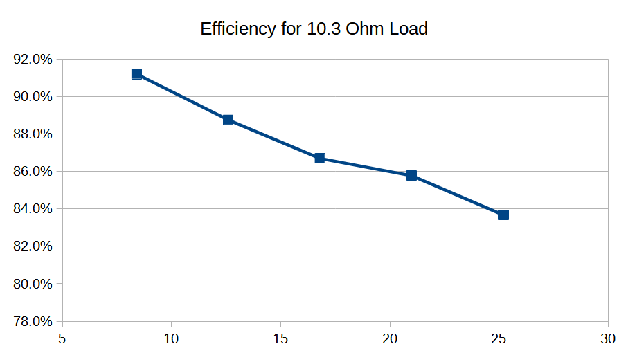
Even before I received PCBs I was working to make it smaller. C1 and C3 changed to an 0402, C2 is now 0805 and rated 35V, C4 is 0603 and rated at 10V. R1 and C3 moved to the bottom side of the PCB to save some space. The inductor changed to a TDK TFM252012ALMA4R7MTAA: 2.5mm x 2mm x 1mm, rated at 1.6A. The new PCB dimensions are 10.3mm x 6.8mm. That's 38% smaller than the first pass. The PCB costs $0.55 for 3 boards from OSH Park, so I'm expecting the total BOM to be less than $0.90 per board.
The weight of this smaller board is only 0.24g (without wires).
I tested this new design with a 1A load. It had an efficiency of 83% with a 25.2V input, but got too hot with no airflow and went into periodic thermal shutdown. It has and efficiency of 85% with an input of 16.8V and doesn't shutdown with a 1A load. I taped a thermocouple sensor to the back of the board and measured temperature with input voltages of 16.8V, 21V and 25.2V. At 16.8V the rise was 40C, at 21V the rise was 50C, and at 25.2V the rise was 61C before it entered thermal shutdown. All measurements were conducted in still air. The thermal resistance of the RY8310 is specified as 105C/W, with a thermal shutdown temperature of 160C.
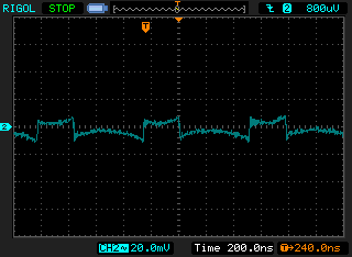
The scope trace above is the output ripple under a 10 Ohm load with an input voltage of 16.8V.
The scope trace above is the switching node of the inductor. Nice and clean.
I still have a few measurements left to perform, but right now I would conservatively rate this converter as 5V/0.5A output power over the 7V-25.2V input range.
Step-Up (Boost) Converter:
Designing a boost converter is more difficult than designing a buck converter (IMHO). The voltages are a lot smaller (at the input), the currents are much larger (again, at the input), which puts a strain on the converter to provide the required currents to the inductor via the switches (either synchronous or non-synchronous).
Case in point: a buck converter with 11.1V input and 5V output has a peak current in the inductor and switch equal to 1.2A, for a 1A load current. Conversely, a boost converter with 2.5V input and 5V output has a peak current in the inductor and switch equal to 2.4A for a 1A load current. Q.E.D.
My primary purpose for this booster would be to supply the VTX and camera with 5V from a single cell Li-ion battery. It would have to supply 600mA @5V while the input voltage ranged from 4.2V to 2.5V.
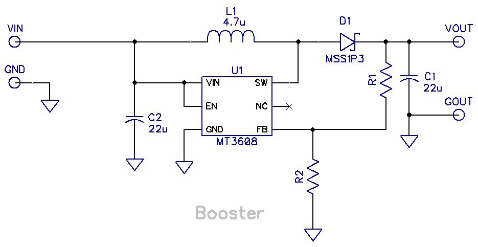
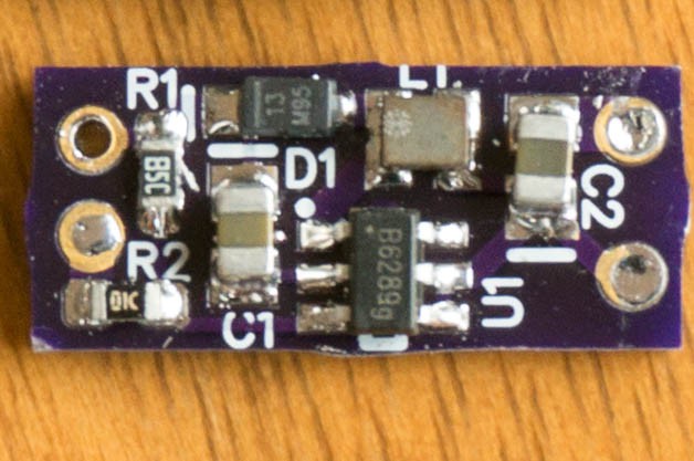
My first attempt at a boost converter used an MT3608 chip and the same 4.7uH, 1.1A VLS201612HBX inductor as the buck converter. I was trying to go really cheap and the MT3608 is less than $0.10 in low quantities. I used R1=75k and R2=10k, which yields 5.1V at the output.
It was small: 15mm x 6.5mm, and light: 0.31g, but could not output much of a load.
The MT3608 chip is a non-synchronous converter (needs a diode for the high-side switch), with a 1.2MHz frequency and an internal 80mOhm (typ.) switch. The data sheet is pretty sparse. It claims that the MT3608 automatically switches from PWM mode to PFM mode at light loads, but it doesn't define what a "light load" is.
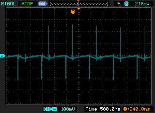
The first test was to just measure output voltage with no load: 5.1V over the input range of 2.5V - 4.2V. Then I put an 8 Ohm load on it (635mA) and things did not go well. It held the output voltage until the input voltage fell below 3.5V and the input current started rising quickly above 1A. At this point the inductor current exceeded its saturation rating and there seemed to be some sort of thermal runaway where the input current ramped up over 1.5A and the MT3608 went into thermal shutdown.
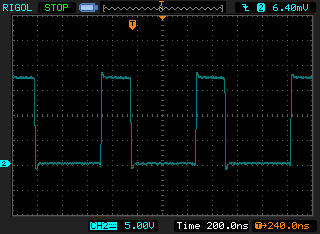
It runs OK with lighter loads. I used 100 Ohm as a load (51mA) and it was able to hold the output at 5.1V with the input voltage at 2.5V. The output ripple is a bit concerning. Here's what the output looks like with the input at 3.5V:
I increased the input voltage to 4.2V and things got worse:
I believe that the MT3608 is operating in PFM (pulse frequency modulation) mode. The MT3608 datasheet doesn't define what PFM is, but I surmise that it is a pulse skipping mode of some sort. There is a minimum duty cycle in PWM mode. If the load requires a duty cycle lower than that the MT3608 will skip a few cycles to drop the load current and then go back to its minimum duty cycle PWM, which causes the current to slowly ramp up in the inductor.
I still need to measure the efficiency of this board, but I'm moving on with an improved PCB layout, which uses smaller capacitors and a bigger inductor to handle more current.
The new board is only 11.43mm x 6.35mm (25% smaller). The capacitors are 22uF 0603, rated X5R rated at 10V. The inductor is TDK TFM252012ALMA4R7MTAA, rated at 1.6A (a 50% improvement in load current) that matches the peak current switch rating of the MT3608. The BOM cost should be in the $1 range.
This design was a bit disappointing. It is non-synchronous, and therefore less efficient than a synchronous switcher, but it can't really operate with the desired 600mA load with an input voltage below 3.5V. The efficiency drops to less than 75% and the output voltage sags below 4.5V as the input voltage is decreased below 3.5V. With light loading (<50mA) it really shines: I was able to decrease the input voltage to 2V before the UVLO kicked in.
Booster for Higher Currents:
I have my doubts about whether the MT3608 can handle a 5V/600mA load with a 2.5V input. So I set about to design yet another boost converter with higher current capability:
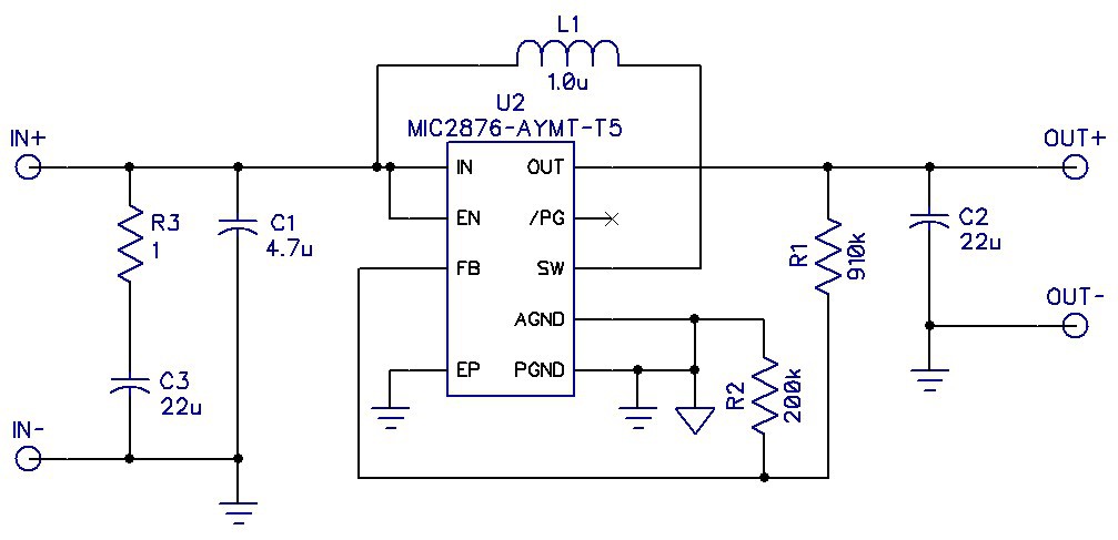
This is a synchronous boost converter using Microchip MIC2876. The PWM frequency is 2MHz, dropping the inductor to 1uH which also allows for increased current ratings in a smaller package. I found a Sunlord WPN201610UF1R0MT inductor, 2mm x 1.6mm, rated at 3.65A (temp) and a sat current rating of 4A. That's a pretty good match for the MIC2876 4.8A switch rating.
The max input/output voltage limit of the MIC2876 is 6V. I added R3 and C3 to reduce the ringing at the input when the battery is connected. Otherwise the undamped ring could blow up the converter.
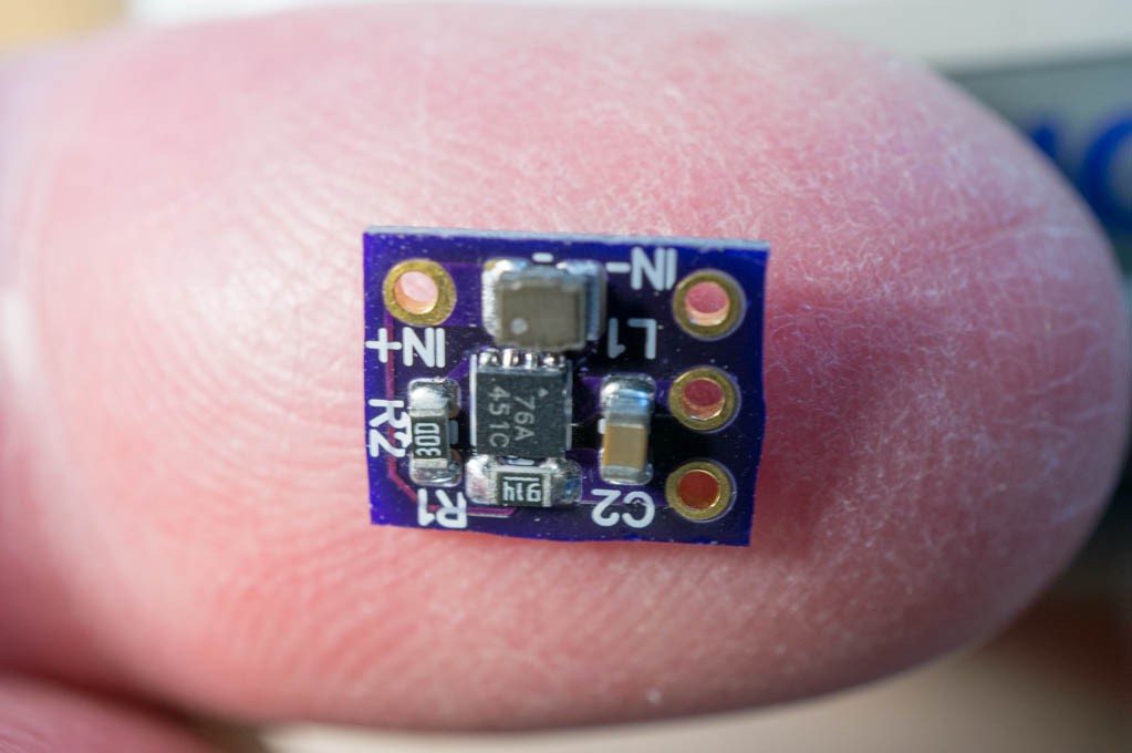
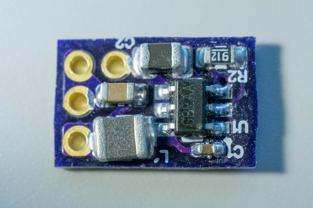
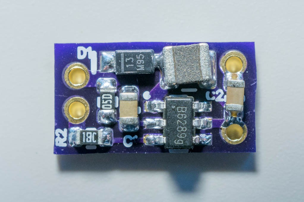
The PCB dimensions are 9.05mm x 7.15mm (ridiculously small!) It weighs only 0.2g without wires. C1 is 0402, C2 and C3 are 0603. R3, C1 and C3 are mounted on the bottom side. The MIC2876 is a very small 2mm x 2mm UDFN package, which precludes hand soldering.
OSH Park charged $0.50 for three PCBs, but I expect this BOM cost to be close to $2.00 due to the $1.20 price for the MIC2876, and $0.22 for the inductor.
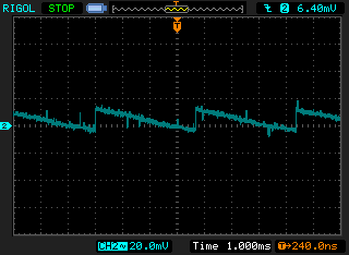
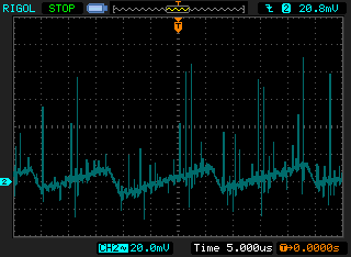
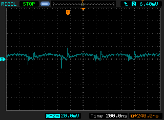
The scope trace above is the output ripple with no load -- in pulse skipping mode.
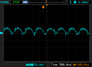
This is the output ripple with a 620mA load.
I tested this board with a 5V/1A load. With input voltages greater than 3.5V it worked well. With an input voltage of 2.5V it shutdown due to overheating.
I decreased the load to 640mA (a 7.8 Ohm resistor) and found that the converter could provide the required output power with an input voltage of 2.5V. But it is a bit marginal -- decreasing the input voltage to 2.4V caused it to enter its UVLO mode. Even so...I think this will work nicely for its intended purpose.