There are multiple implementations of such converters for high power applications both in isolated and non-isolated versions [https://www.ti.com/lit/ug/tiducs2b/tiducs2b.pdf] [https://www.ti.com/lit/ug/tidud04/tidud04.pdf] . Quite often in my battery powered project I face a need to develop both a battery charger and the converter stabilizing the battery voltage. The possibility of joining those two converters allows for savings on power elements and size. I wanted to try to develop experimental board to test different current measurement circuits and try to push the limits of maximum power. In this article I will try to present how to build a simple bidirectional converter with fast primary current feedback loop and digital secondary voltage feedback all implemented with small 8bit microcontroller.
Topology
In presented design I’ve decided to join two classic non-isolated topologies the buck and boost converter. In this configuration the converter allows for transfer of energy between two voltage potentials in both directions.
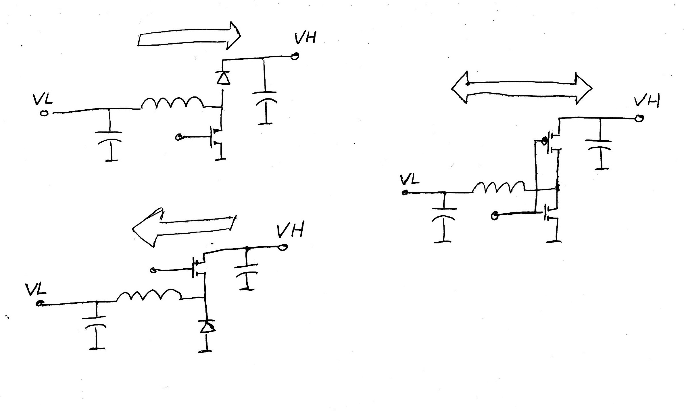
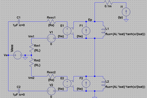
In such converter control of current flow is not only dependent on the PWM signal but also on the ratio of input voltages. Creation of feedback loop which only maps input voltages to the PWM signal would not only be difficult but also hard to stabilize. Also it would omit control of the current where current is one of the most critical parameters in charging and discharging of batteries. Probably because of that problem most of the mass produce converters for charging include feedback loop measuring current flow trough small resistor in series with the power inductor. This arrangement allows to measure current rise and fall at each cycle of the converter. Considering different possibilities of measuring that current I sketched following schematic.
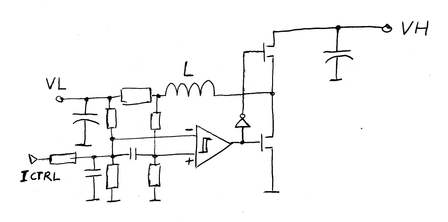
In presented circuit the main feedback element is the voltage comparator with hysteresis. By defining the converter phase and the state of main transistors it determines the cycle of increase and decrease of current in the main inductor. By simultaneously monitoring the current in the inductor trough the feedback resistors it limits the maximum rise and fall of that current. In this combination a negative feedback loop is created which creates cycle-by-cycle oscillations maintaining the inductor current within predefined range. The oscillation frequency is not fixed and it depends on inductor and resistors values, input voltages and and comparator hysteresis. Although the converter oscillates, in it’s default state the average current flow trough the inductor is null and no energy is transferred. Such oscillations maintain inductor in continues conduction state which might appear wasteful because of elements parasitic RI losses but surprisingly in presented circuit such losses represent only around 1Watt. While the comparator maintains the inductor current within predefined range additional control input (Ictrl) injects offset to the current measurement forcing average current to deviate. This allows the control of average current flow between input potentials and creates a abstraction block of voltage controlled current source.
Basic design
The main obstacle in designing bi-directional
converter is not
only a need for
controlling the voltages at the input and output but also the
decision of direction and amount of
current flow. That is why most design are
based on a digitally
implemented feedback loop inside a
microcontroller or a
dedicated DSP. To simplified my design both
in circuit and in software
I decided to use a simple
8bit microcontroller, consciously
sacrificing final precision and reaction speed for cost and
simplicity. I decided to use the Attiny1616
because I contained all necessary peripherals in a
simple package. Bellow is a diagram of the
converter design in it’s
initial form.
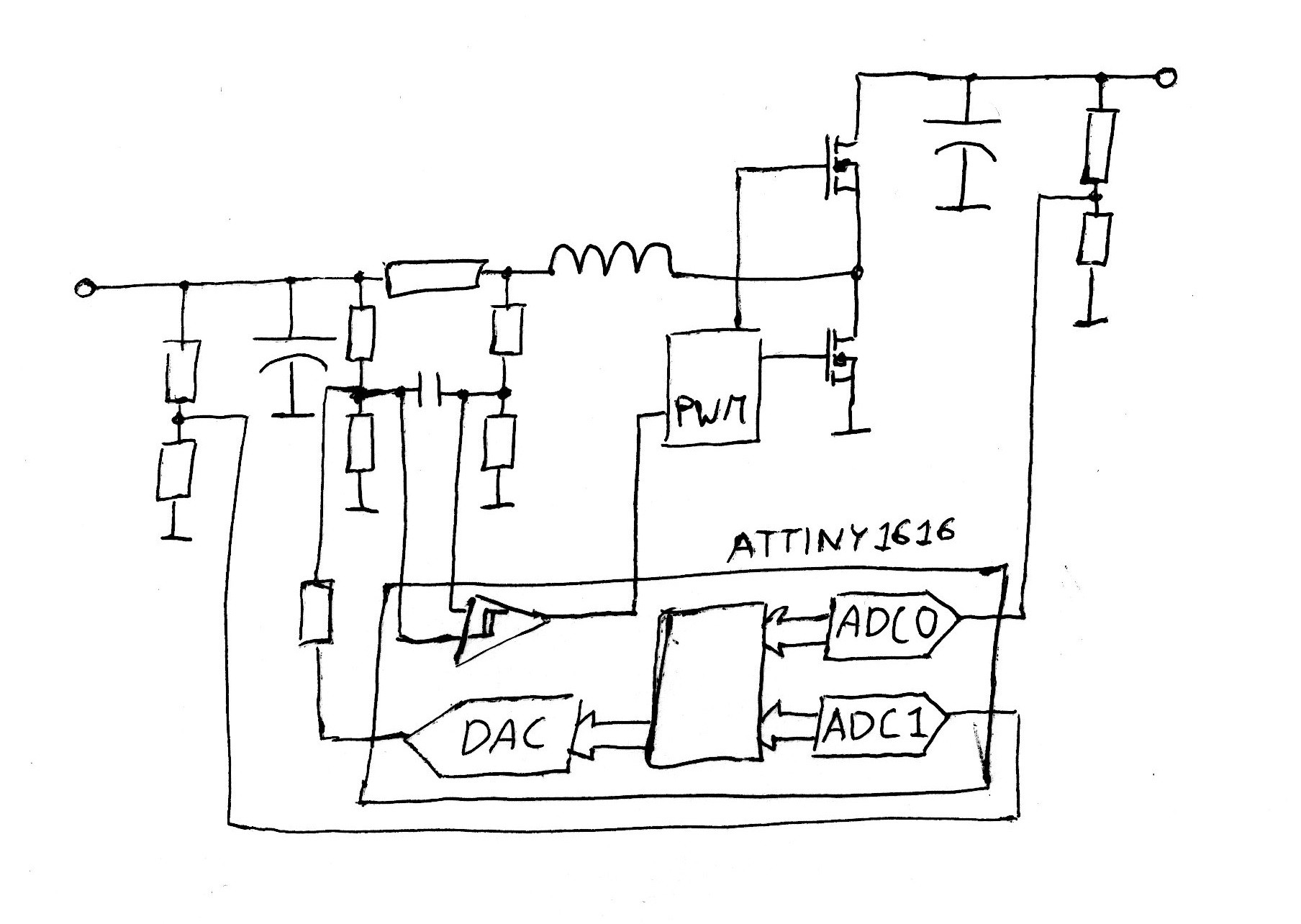
As I mentioned the main feedback loop creating oscillations and controlling inductor current is based on comparator with hysteresis. Using the build-in comparator...
Read more »
 jbb
jbb
 CentyLab
 Marc-O.
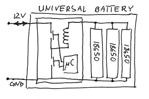
So here's another use case I have:
I use a 36V ebike battery to power high current (20A) radios. These use an LT3800 synchronous buck convertor from aliexpress which is actually pretty well made, and works very well.
It would be nice to be able charge the ebike battery from the car.
Perhaps I can switch the gate of the low side fet onto a boost controller to get charge mode. As long as you keep away from saturation (and this is a 20A inductor), then boost only requires predicted timing based on Vin, and no pulse by pulse feedback, and no current sensing. So the micro could drive charging, and leave the LT3800 to control buck (which it does well with its nfet bias generation, fast fet drive, power regulator, and so on).