 agp.cooper
Modelling the Flip Coil
Here is a schematic based on Mirko Pavleski's Pulse Induction Metal Detector (PIMD) (https://hackaday.io/project/176291-diy-simple-sensitive-arduino-metal-detector):
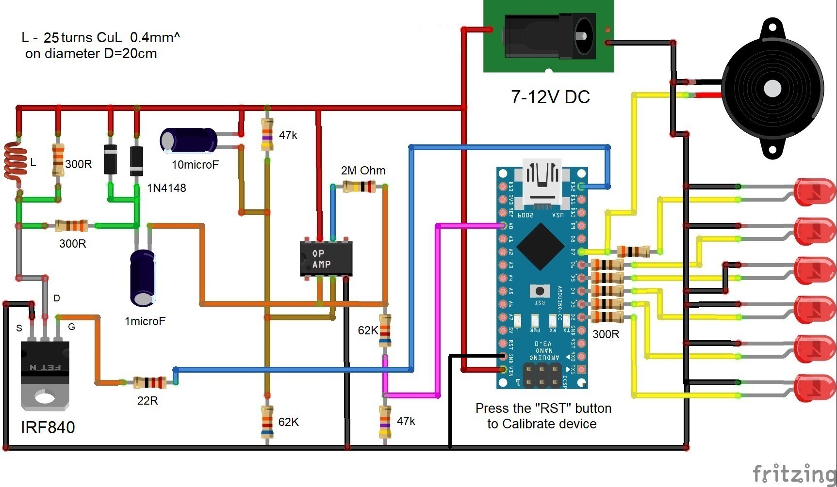
(Note: I think the 62k/47k output resistor divider should be moved from the inverter input of the op-amp to the output of the op-amp?).
Mirko's design really appeals to me because of its simplicity.
The main problem I see is that power supply is not isolated from the inductive voltage spikes from the coil. It would work with a low internal resistance battery but an electronic power supply could be a problem. There is a risk that the inductive voltage spike could be upset and/or damage the op-amp and/or the Nano.
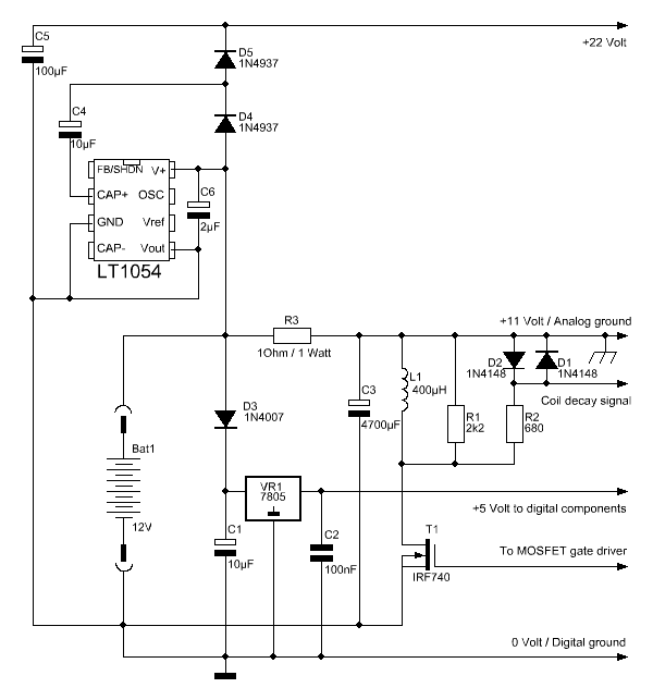
Here is Lammert Bies' PIMD (https://www.lammertbies.nl/electronics/pi-metal-detector):
My favourite however, is the "Flip Coil" by JorBi (https://www.instructables.com/Arduino-Based-Pulse-Induction-Detector/):
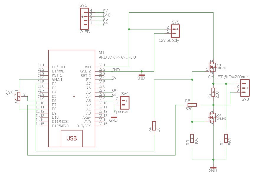
Here he uses R1 to ground the negative inductive voltage side of the coil during the receive period. He also isolates the coil by switching off both MOSFETs during the receive period. This is very clever!
He also uses the ATMega's analog comparator to time the decay of the signal to reference voltage (40mV). Rather than the analog to digital converter (ADC). Again, a very clever solution.
Some notes/faults with his design are:
- No protective diodes for the Nano (he relies on the Nano's internal diodes).
- No power supply decoupling. Risk of inductive voltage spikes upsetting the Nano.
- MOSFET Q2 should have a higher breakdown voltage to shorten the coil current decay. I would use an IRL740 (400v) or an IRL840 (600v) or equivalent. MOSFET Q2 has to be an IRLXXX type in order to be directly driven by the Nano.
- MOSFET Q1 really does need to be an IRLxxx version to minimize the voltage drop across the MOSFET.
- Rather than use D8 to power the reference voltage potentiometer he should used the Nano 3v3 voltage supply.
- The speaker line should include a 220R current limit resistor.
- The I2C lines should have 4k7 pull up resistors.
MOSFET Types
As I was researching this project it took a while to realize that there are "normal" MOSFETs (i.e. IRF540) with a gate threshold between 2 and 4 volts (read 4 volts) and "logic" MOSFETs (i.e. IRL540) with a gate threshold between 1 and 2 volts (read 2 volts).
In my case I used an IRF540 and an IRF740 until I realized benefit of using the IRLxxx series for this application. Unfortunately I had already sent of a PCB for manufacture.
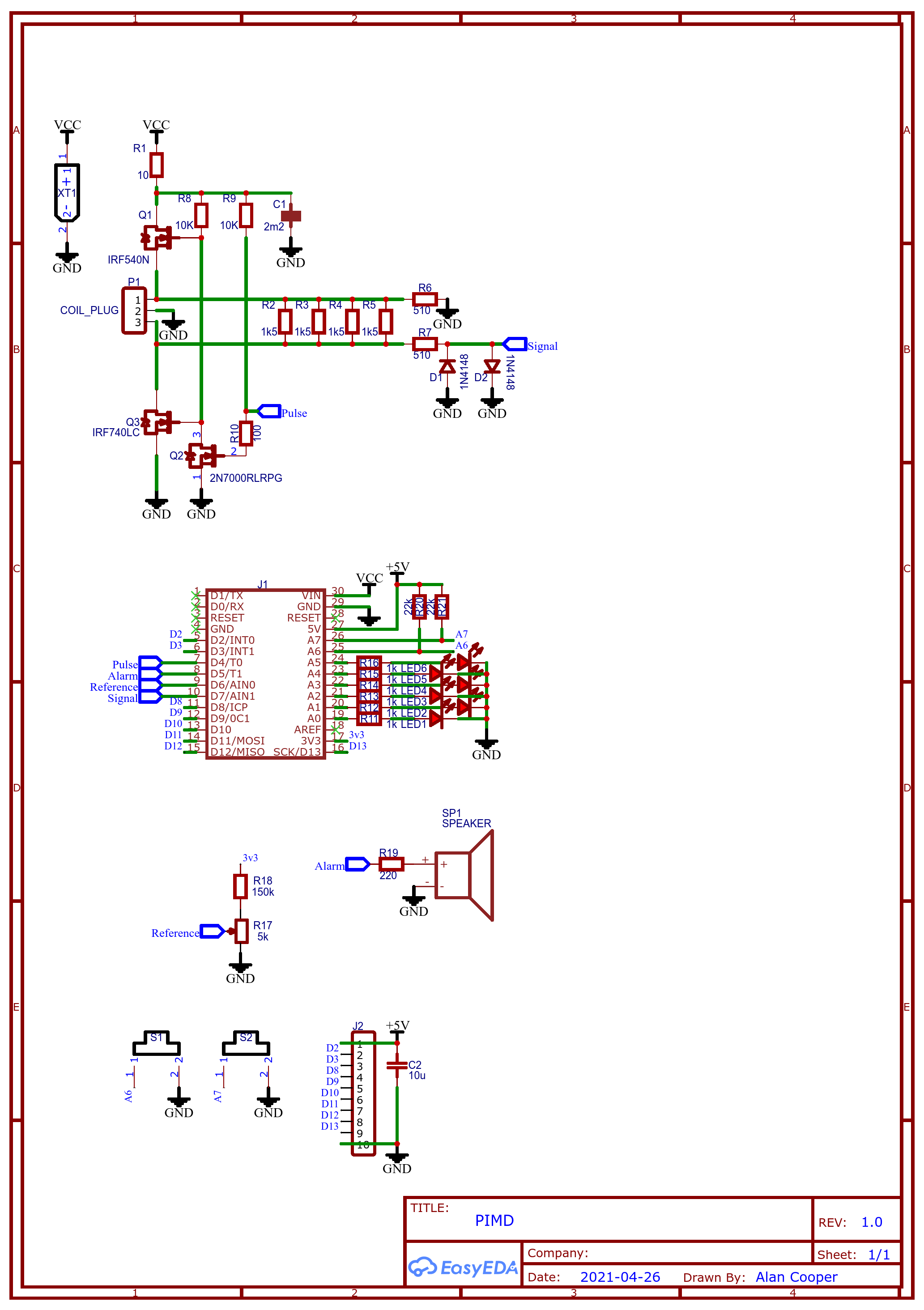
- A direct XT connection on the PCB for 7.4v or 11.1v rechargeable LiPo battery packs.
- A logarithmic LED display.
- Not immediately obvious are two switches that use the often unused A6 and A7 pins of the Nano. To use these pins, an analogRead() is required:
// Check for power down and restart loop();
if (analogRead(A6)<=511) {
while (analogRead(A6)<=511); // Wait for buton release
delay(20); // Wait for debounce
Start=false; // Set flag off
}
- I have used four resistors (1k5) in parallel to increase the power dissipation.
- Because I am using the IRFxxx series MOSFETs I have to drive the power MOSFET gates from the high voltage (>5v) supply. Thus the 2N7000 MOSFET gate driver.
- The gate driver requires an inverted logic from the Nano (i.e. normally high (off), pulse low (on)).
- One of the switches (i.e. On/Off) will be used to power down the Nano rather than disconnect the power supply.
- The other switch (e.i. Mode) will be used to toggle between to configurations.
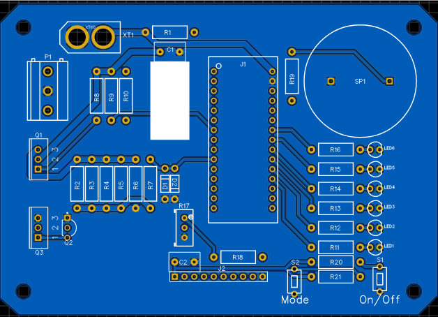
My PCB Layout
Here is the board I sent off to be made:
Modelling the Schematic
I used TINA to model the schematic:
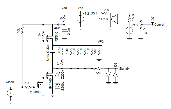
The spice models have limitations, one being the MOSFET breakdown voltage, thus the two series zeners across the IRF740.
The schematic has been optimized to determine the resistor values for critical damping of the signal.
Checking the voltage drop over the power MOSFETs indicated that the IRF540 needs to be upgraded to an IRL540 type. The voltage drop across the IRF540 was about 4 volts, while the voltage drop across the IRL540 would be about 2 volts.
Here is the modelled receive signal (coil voltage decay only):
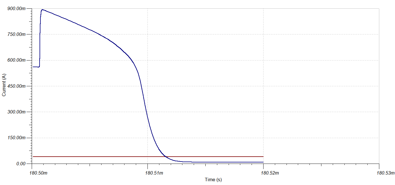
The graph shows a critically damped signal (blue) and the 40mv threshold (red). The initial jump up just after 180.500 ms is the coil pulse being switched off and limited by the protection diodes. The modelling suggest that the coil voltage decay will be practically zero after 14 us.
The Target Signal
What does the target signal look like? This image is from Jozef Froniewski of Silego Technology
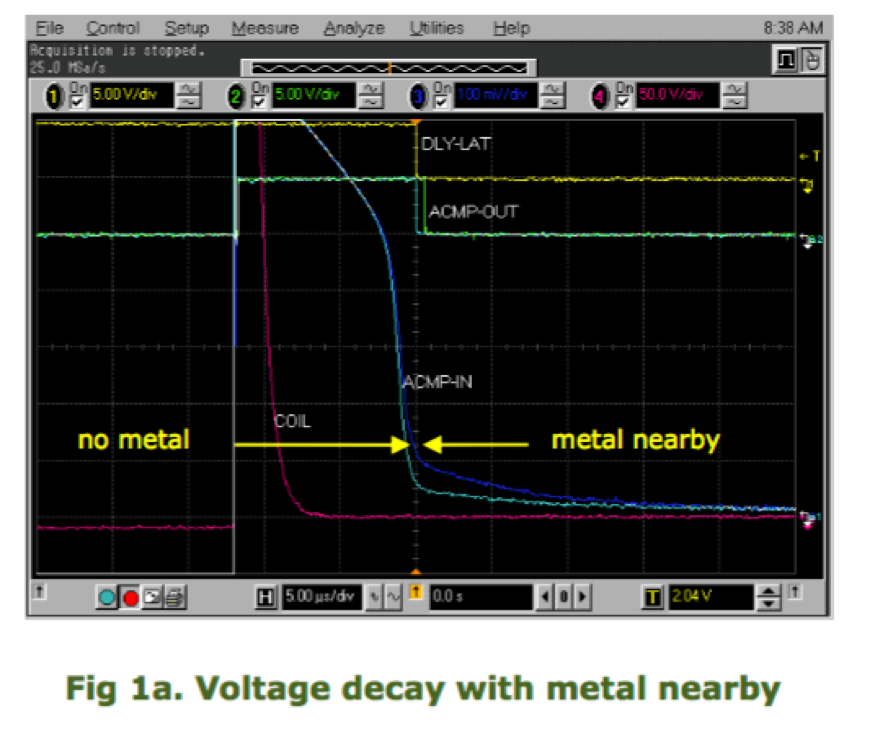
Note that the "no metal" curve maps reasonably with my modelled curve.
Ground Effect
Although Corbyn in his March 1980 Wireless World paper states he had not found any gold with his PIMD, he did find several nuggets up to 1 oz in size by 1981.
His design looked at removing the "ground effect" of the iron rich lateritic soils of the Eastern Goldfields of Western Australia. He modelled the ground response as:
g(t) = A*((1-P)*exp(-t/T1)+P*exp(-t/T2))
where:
A = signal amplitude
P = 0.08 to 0.3
T1 = 0.75us
T2 = 550us to 800us
Here is a graph using mid values for the parameters:
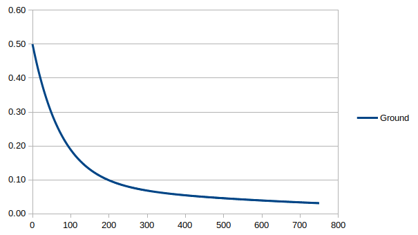
Clearly, in Eastern Goldfields the ground effect will swamp everything other than a "large" target.
In those days I did look at using an i8085 as a base for a ground effect discriminating PIMD based on Corbyn's paper, but technology, and my resources, knowledge and time were not adequate for the task.
To take on ground effect discrimination would require using the ADC, which is not the focus of this project.
AlanX
Discussions
Become a Hackaday.io Member
Create an account to leave a comment. Already have an account? Log In.
One thing I found very interesting when modeling the coils it to also model the target -- If you add a matching coil and coil resistance (a floating loop), and link them (like with a Spice ".K L1 L2 1" transformer constant,) you can easily vary the target coupling (or target material by varying the coil inductance and resistance) and see how the circuit responds.
Prototyping-wise, if you make an identical coil and short it through a pot, you can experiment with how well the impedance of a target matches the detecting coil.
Are you sure? yes | no