 gilphilbert
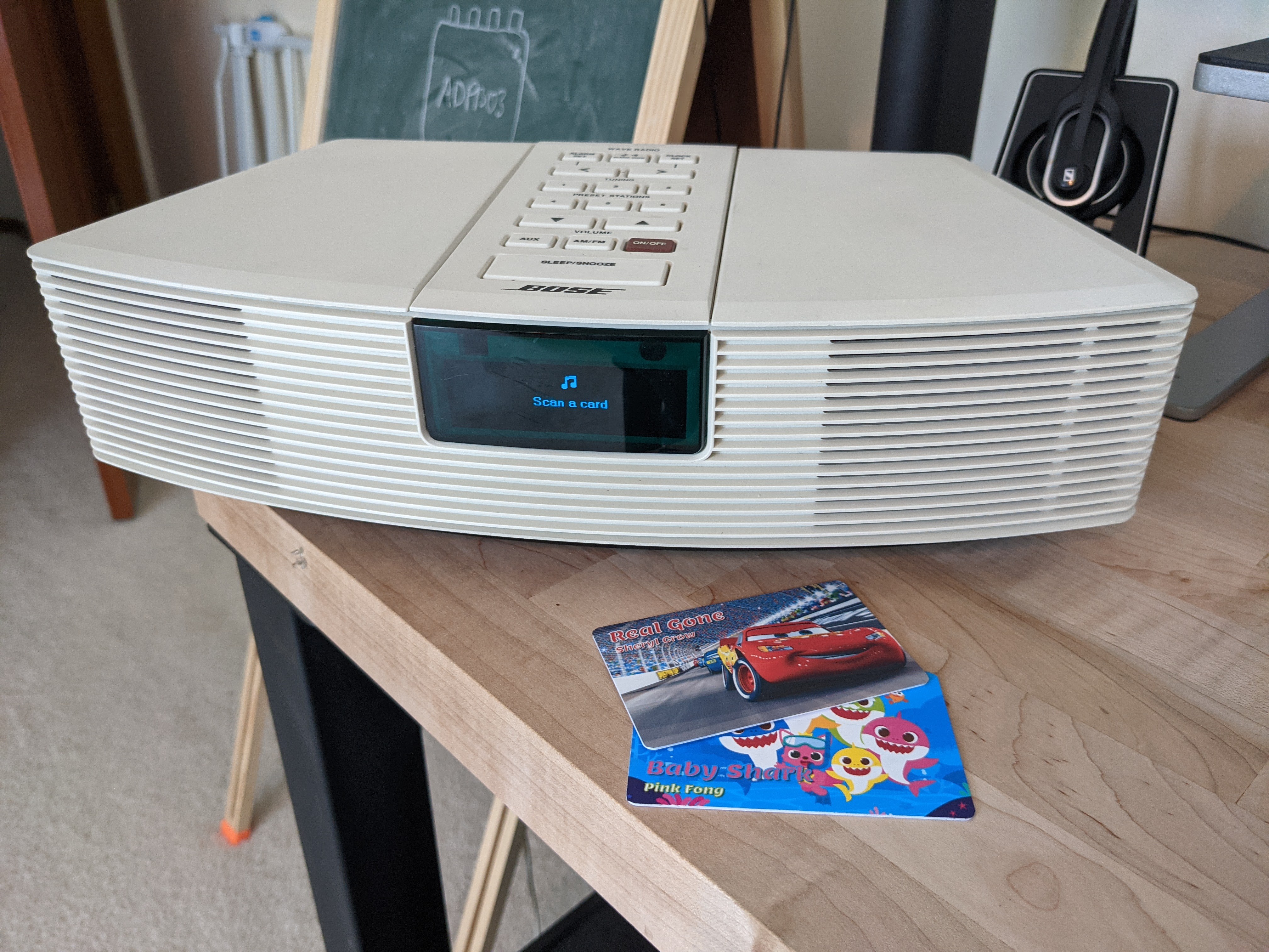
After deciding I was actually going to do this, I had to select a radio that I could gut completely - I needed it to have enough space inside that I could fit all my new hardware and space for a display. I also wanted something with a few buttons so I could have volume control, programming new cards, etc. I also wanted something that wasn't too painful to my ears (I can't stand cheap radios). This is for my kids, so audiophile isn't required - but something that I can stand, at least.
Really, I just wanted something my kids can use that can take a bit of a beating, doesn't cost the earth, isn't painful to listen to and can fit everything inside.


 Jeff Cooper
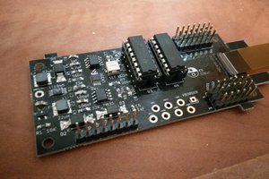
 sapir
sapir
 bobgreenwade