 Eric Hertz
well.... this page suggests absolute-addressing does some funky stuff...
http://jgmalcolm.com/z80/variables/abso
The table suggests RAM starts at 0x0c000 (which is where the first page is always "mapped"), but, thereafter continues unbroken (in 24bit addressing mode) all the way through the 128KB to 0x2bfff. NOW, where's that leave the ROM?
From what I've pieced together, the ROM is then sequentially addressable from 0x00000 to 0x00bfff... which means only 48K of the 256K of ROM is accessible via 24-bit "absolute" addressing. That can't be right... can it?
I guess the thought could be that there's no reason for fast bulk copies from ROM... and execution is really only possible through mapping, since the instruction grabber is only capable of 16 address bits... but, still, this seems weird.
The actual logic to do it this way is not much less, maybe even more complicated than, say, treating the first four pages as always remapped from different addresses. E.G. the highest "absolute" address bit (A23) could select RAM if high, ROM if low, then 8MB of ROM could be accessed sequentially and 8MB of RAM, thereafter, starting at absolute address 0x800000. The actual mapping logic to permanently map the first 16KB from 0x800000 to 0xc000 is actually identical. In fact, I'm pretty certain the necessary circuitry would be LESS to do it this way... and it shouldn't mean any different instructions, either.
So, I think I must be missing something...
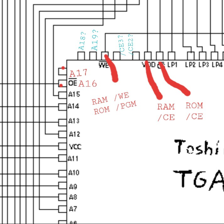
Earlier I noted that there may in fact be two more chip-select outputs, and that wouldn't fit this scheme. Maybe they're just address lines.
Which brings me to the point in the project where a logic probe and custom test software would be in order... and you know how likely this endeavor is to wipe the memory with a minor slip of the probe... and how much effort it is to reload, in my situation. Now devel on a laptop, even just for each measly pin-test program, seems the way to go. :/ why I gotta be a hardware hacker? It'd be so much easier to write games under these conditions!
So, that's my guess BEFORE absolute-addressing...
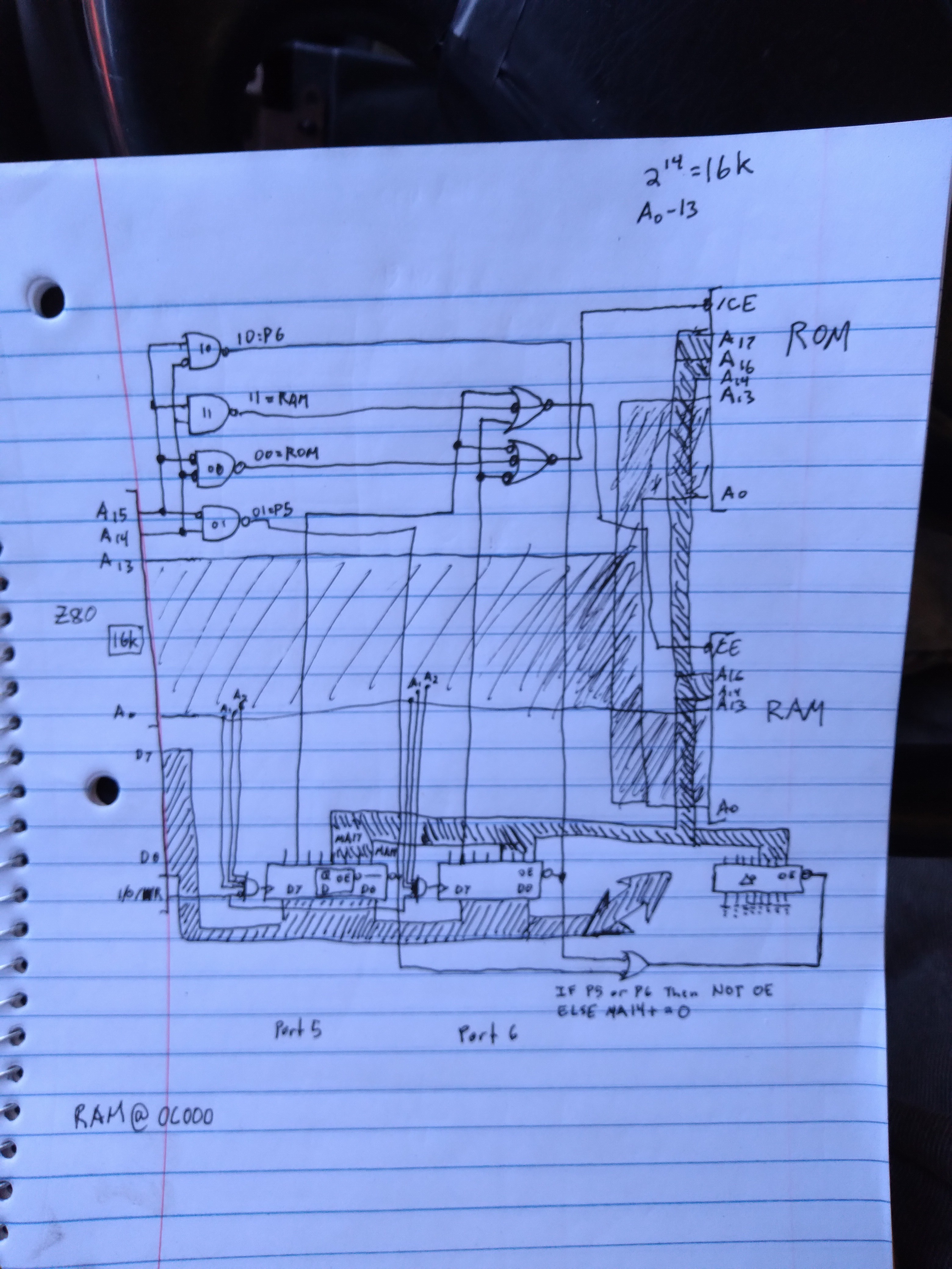
And this hokey ugly mess is almost what makes absolute addressing work to match the table... except there has to be an additional bodge to disable mapping for absolute addresses below 0xc000... where's that signal coming from???
A16-23 I could see coming from a Port... but, no, again with the Von Neuman architecture... you can't hold that on the address lines from an out instruction, because the next instruction has to be fetched from the (same) 16bit address bus... so something has to indicate When to use the 24bit address... a signal that isn't typical Z80, no? Unless... hmmm... maybe say all the 24bit instructions are all the same length... e.g. they're all actually 16bit instructions 3bytes long, then a counter external to the Z80 could wait to output the high address byte until three bus-transactions later (and disable it after the fourth)...
I guess I'm intrigued how this could be implemented with a regular z80 processor where internal signals like the A register or some sort of timing-signal are not broken-out, and no special instructions are added... an add-on for other systems... I'd never heard of direct-addressed paged memory... swapping the pages seems time consuming... though, I suppose such is probably implemented in most expanded memory systems.
....
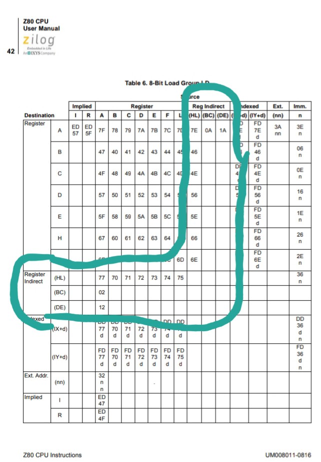
Ahhh, but look here... These instructions are all one byte long, and could be used to accomplish all the goals...
So, then, the high byte of the address gets loaded to a d-ff on a port via an out command, then it's delayed by one bus transaction before being output to the actual address bus, e.g. via output enable attached to a DFF used as a single bit shift register clocked by, say, the MEMRQ pin. (Which isn't necessarily available at a pin on this chip). So the high byte of the address is available *after* the cpu reads the next op-code (ld reg, (addr) or ld (addr),reg) which is just in time for the ld instruction to stick its 16-bit address on the bus, right alongside the extra address bits. And, finally, that delayed /OE for the high address byte *also* disables the other address-drivers, such as the memory-banking... and then it's automatically cleared back to normal after the access. Not bad...
Alternatively, was thinking maybe assembly can use the assembler's pseudo-program-counter (e.g. as used to calculate distances for relative jumps) to load two bits into the port, indicating the delay... but that'd require either another out instruction, or masked-writing and would reduce it to 22bits of address... though, separate port-writes, to different port addresses, indicating the delay.. hmmmm.... port 0x11 = 1 delay for a single-byte opcode following, 0x12 for a two-byte opcode... hmmmmmm.... and, again, could the assembler calculate that and add the 0x10 automatically?
So... what uses has this over mapping...?
Just a single byte load each time... great for grabbing or putting a value quickly from/to somewhere... maybe ideal for global variables or circular buffers awaiting slow transmission... but if accessing numerous values regularly then remapping is obviously faster. Ahhh, perfect for memory-mapped I/O...
Yeah, I think it's useful, eh?
Oh, ALSO, this enables actually 24bits of address space, whereas the mapping system can only map 19bits (including one to select ROM/RAM), or 21 if those extra unknown bits 4 and 5 in the port registers are actually address bits, or 22bits at best if it's as I think and bit 7 in the remap ports is also used to select other chip selects.
LOL, BAH!!! INTERRUPTS.
....
OK... this, I don't think matches the TI-86 absolute addressing system, but could be a way to implement something useful. The bank mapping is the same.
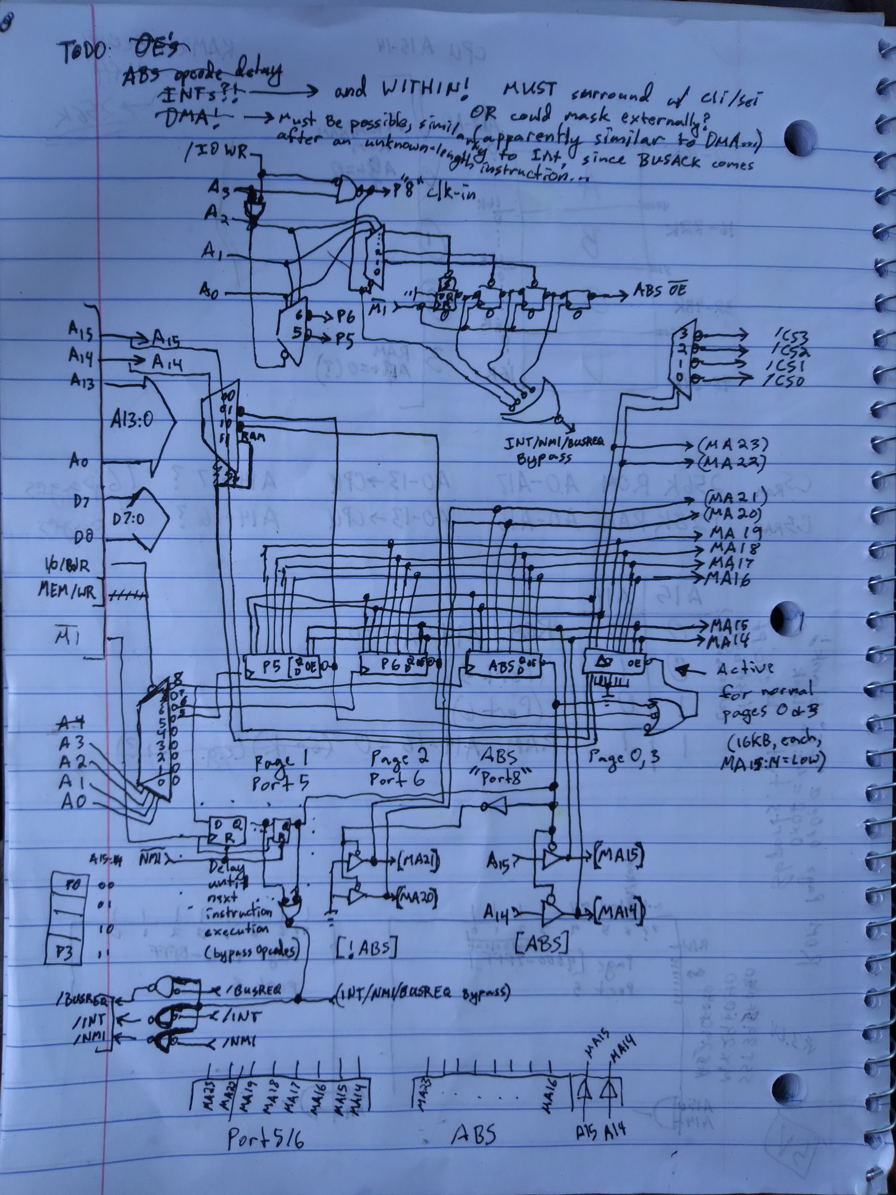
The upper portion replaces the dotted-portion at the bottom "delay until..."
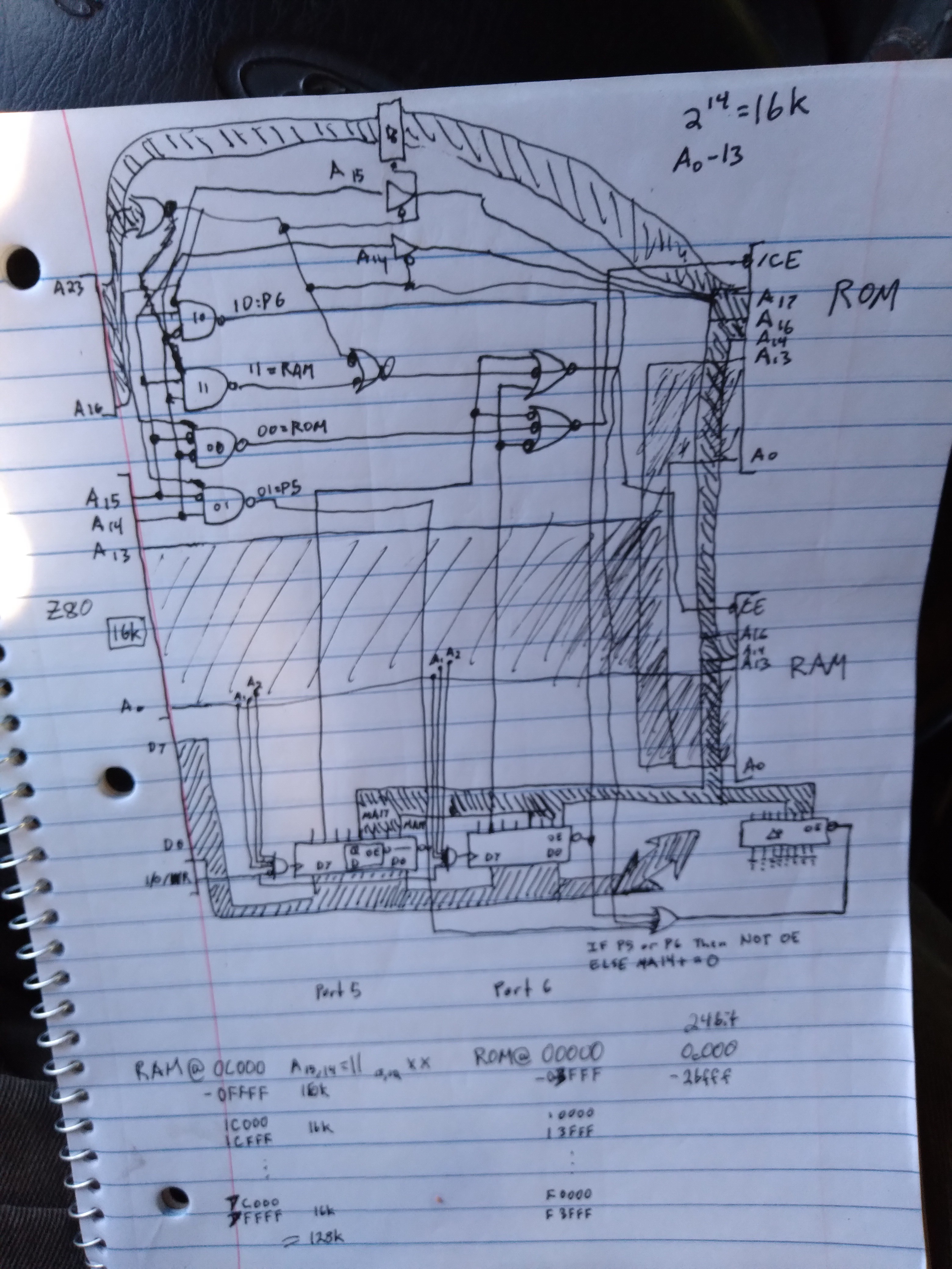
So, Normally, it acts the same as the TI-86's bank mapping, but also allows for mapping up to four memories (via separate chip selects, addressed by port5/6 bit 6 and 7) whic can each be up to 20 address bits in length (1MB?). The lowest 16KB of ROM and RAM are still always mapped to 0x0000 and 0xC000, as before, except during absolute addressing, which completely overrides the normal mapping scheme and can access the four memories at up to 22 address bits, (4MB?) each. The upper 3MB of each cannot be mapped, only accessed via absolute addressing. The four memories are chip-selected by A23 and A24.
Now, Absolute addressing is done by first writing A16-23 to "port8" (I shoulda done "port10" instead, let's pretend I did), then writing the upper address byte to port 10 basically disables absolute addressing ( prb unnecessary). A write to port11 delays the absolute address for one M1 cycle, port 12 delays it for 2 M1 cycles, etc. Meaning: say the next operation, after the port-write, is a load from an absolute address to register A... That opcode (load from a 16bit address to A) is one byte long. So, using Port11, with a delay of 1 would cause the absolute addressing to wait for the one byte opcode fetch, then the 24bit absolute address will be used instead of the 16bit mapped address during the next bus access, which is to load the byte. If the next opcode is two bytes long, then write to port 12 instead.
I guess that's about it.
Realistically, it's not just the opcode byte count, because I haven't really looked into the opcodes enough to determine whether, e.g. one exists which performs two memory accesses. In fact, I think I recall seeing a "search" which goes through many addresses sequentially... could such be as simple as latching the absolute "delay" at the last register until the next M1?
And, in such a case, there's no incrementing across the lower 16bit address boundaries.
These CISC machines be CRAZY!
Now, I'd completely blanked on the need for atomicity, earlier... but I think it should be OK to just bypass the NMI, IRQ and BUSREQ signals until after the absolut-addressed instruction completes. As far as I can tell, that's exactly what the CPU does internally. Maybe i need to latch them, first, then bypass with an OE on the latch, if they're short pulses, or edge-triggered. Regardless, as far as I can tell, none of these interrupt an instruction that is presently executing, and some can execute for quite some time, so a delay of one extra (comparatively short) instruction shouldn't be a problem AND doesn't require extra instructions to e.g. read the interrupt-enable bit, clear it, then reenable it afterwards (if necessary).
This really seems quite doable... And doesn't really require a whole lot of extra circuitry. And, in fact, fits within the unused/unknown pins surrounding the known high address bits and the two chip selects for RAM/ROM, And doesn't require access to signals internal to a regular Z80, nor special instructions, And fits within the functionality of the paging system...
Since I haven't found much in the way of information regarding HOW 24bit accesses are actually implemented, this would seem a reasonable-ish assumption, if it weren't for that weird bit about the RAM's allegedly being absolute-addressed from 0x00c000 to 0x02bfff... which, again, seems like it would take *more* circuitry to implement.
And, depending maybe on the assembler, it might be doable to automatically choose the appropriate "port" to write... e.g.
Ld hl, 0x1234 ; ahl = 0xf01234
Ld a, 0xf0
Out next+0x10, a ; write to port 0x10+opcodeLength
Ld b, hl ; get the value at ahl and store in b
next:
; do something with the value
...
Now, I keep getting fixated on the idea of "latching" absolute-addressing for multiple accesses, like a separate type of page mapping, but I dunno... maybe disable during /M1 is all it takes?
Heh, and /now/ fixated on whether this could also be extended easily to be used as another sort of paging system, wherein everything runs in a 64k page set once by say port 0x1f... (how, then, to access things outside the page and return?)
HAH, and NOW fixated on the idea of /mixing/ the two paging systems. E.G. maybe the upper address byte stays, the entire ROM/RAM can be copied to an otherwise only absolute-addressable portion of RAM in the upper 3MB, and then the normal paging system works within that. The only thing is, port5/6 uses a bit (possibly two) to select between ROM and RAM... so, presently, this'd still access ROM, just at an offset set by port8, which is of course not loaded with anything, or even misaligned. (Is that why bit 6 was used, instead of 7?)
And then, of course, there may become a bit of "nesting" which would overwrite port8 (10, dagnabbit!) so maybe a port20 with an additional register...? Anyhow...
I guess part of the reason this intrigues me is all the stuff I've done with SDRAM, when working on those projects I often wondered about throwing a stick of 16MB or more at an older system like this, and how to make use of it. Some of the synchronous aspects seem difficult to work with in an asynchronous system like this, but sdram has some extra functionality that makes it seem less-so. E.G. if you hold a "read" command on the bus for MANY clock cycles, it will just keep outputting that same address, very similarly to static or dram. Thus, it could be clocked far faster than the CPU, and MOSTLY appear asynchronous, like any other memory a system like this was designed for, except for a few minor details which I'd been mulling over for some time. #sdramThingZero - 133MS/s 32-bit Logic Analyzer was /sort of/ related.
...
OK, wait a minute, in the last log I came up with this... so, it could have 20 address bits accessible, with 4 chip selects, making for 22 address bits, or even 22 address bits and two chip selects making for 23 address bits. It's also plausible the RAM/ROM OEs are on address bits of their own, which would make for 24 address bits accessible externally... but then how would it be mapped? The port 5/6 mapping registers could use bit 6 to select between e.g. 0x400000 (RAM, high bit DISABLES ROM) and 0x800000 (ROM), I suppose... that'd treat the highest two address bits as though chip selects (mutually exclusive). I suppose, then, it could also be possible to use bit 7 to e.g. make those address bits act more normally rather'n mutually-exclusive...
7 6 | A22 A23
0 0 | 0 1 TI-86 ROM selected
0 1 | 1 0 TI-86 RAM selected
1 0 | 0 0 \ address decoding
1 1 | 1 1 / circuitry necessary
That'd be some forward-thinking that probably didn't go unthunk, considering the first devices this chip was used in didn't use many of these extra address pins which were much later used by the TI-86...
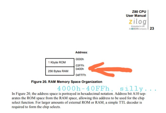
I'm increasingly less convinced the table of absolute RAM addresses makes sense.
And, that table, above, mapping A23,22 could be as simple as merely inverting A23's output to /A23, which would place ROM at 0x000000 for booting and RAM at 0xC00000, WHICH looks suspiciously like the alleged 24bit addressing table, if someone wasn't careful in transcribing... and was thinking about the paging system while doing-so... HMM...
But... that'd mean A22 and /A23 are out of order on the pinout... it might make more sense, then, to invert /A22? I dunno, ROM at 0xC00000 makes less sense (RAM at 0x000000) or does it...? ROM is typically smaller than RAM... and in such systems, executing From RAM is usually preferred (faster). E.G. as I recall, the ROM BIOS on a PC XT actually boots from some high address, then can get copied to RAM... Hmm, I dunno. Intriguing, though, maybe an intermediate step between typical 8bit and 16bit designs...? And, I think, maybe part of the reason for starting at a high address has to do with the reduced address decoding logic necessary, in tying the highest address bit essentially directly to the device, then copying the device to RAM, then just disabling the device thereafter...? I dunno, lots of rambling. TODO Where does the Z80 start from, anyhow?
...
Looks like 0x0000, but that'd be easy to map to with their paging system.
Here's a prime example of how easy it is to get confused...
...
Lol, and ironically, i think i confused A22 and A23 in those ramblings.
A23 (assuming the address bits are in order on the chip pins) is connected directly to the ROM /ChipEnable, and A22, then, to the RAM's. So, the table should be:
7 6 | A22 A23
0 0 | 1 0 TI-86 ROM selected
0 1 | 0 1 TI-86 RAM selected
1 0 | 0 0 \ swappable, address decoding
1 1 | 1 1 / circuitry necessary
Then A22 might be output as /A22 and the RAM would be at C, ROM at 0, Or A23 might be inverted and RAM at 0, ROM at C, or both inverted, ROM at 8, RAM at 4...? Or, if no inversion, ROM at 4, RAM at 8... and either way, the port5/6 decoders for bit 6 are far more complicated than merely feeding out one chip-select and its inverse, right? Though, doing-so might save some external circuitry in many cases, the fact is this RAM has both a /CE and a CE, so could've just as easily tied the RAM CE to the ROM /CE... unless... they had more in mind...
Discussions
Become a Hackaday.io Member
Create an account to leave a comment. Already have an account? Log In.