 Eric Hertz
I think I've worked it out... and, frankly, I'm surprised not only at how easy it should be, but also some inherent factors of the system design that should make it even easier.
First-off, we're talking /full/ RAM backups to FLASH... why? Mostly because I've little interest to try to learn about TI's variable system, which I think is also responsible for storing programs, etc.
Again, this endeavor is, to me, little to do with the calculator's original functionality, and more to do with what new ways it can be used. One of which, for me, is learning about Z80's and Von Neumann architectures, which applies to /many/ systems... wherein TI's OS is useful and a learning experience in itself, but learning /it/ is a bit less useful.
All that to say, the backup FLASH will pretty much simply duplicate the entirety of the RAM, stack, variables, running program, other programs, text buffers, frame buffer, and all. Why not?
Restoring from a memory-clear, then, is simply entering about 6 hex values and running it through AsmComp() then Asm().
Basically it amounts to: Load FLASH Page 0 ("RAM" page 8) into the "RAM" page slot, then jump there. And that's it. I think 6 bytes, 12 characters to enter by hand, total.
Now, once it jumps there it begins executing the real program, which, simply, copies the entirety of the FLASH to the entirety of the RAM, byte for byte.
But wait! That'll overwrite the stack and stuff already in the RAM! ...And? Once it's restored, it should basically act exactly like it did once the original backup was completed.
So, then, how am I going to know where in the backup to find the recovery-app to jump to in the first place, if I'm not going to learn about TI's variable lookup table, etc.?
OK, so dig this: The backup and restore program are one and the same. Running the backup program loads it into _asm_exec_RAM. That means the program is loaded and running from there WHILE the backup of the entirety of the RAM is performed, including a backup of the running program /as loaded into RAM/.
Thus, When Restoring, we know exactly where to jump in the backup image to run the restore program from within the backup image itself.... (_asm_exec_RAM - 0x4000). Minus 0x4000 because _asm_exec_RAM is in RAM page 0, which is at z80 page 3, but the FLASH page 0 will be mapped to ... actually, I should probably map it in the "ROM" section, z80 page 1, so minus 0x8000, since we'll need to map all the pages from RAM to back them up.
But wait! If you're executing from FLASH, then how you gonna switch in the FLASH pages to backup to/restore from?
Ahh, but see... The first step is to copy the first page, which happens to contain _asm_exec_RAM, which is always mapped in at z80 page 3. So, after that first page is copied, we resume execution not from the FLASH, but from the duplicate now where execution normally happens, in the RAM.
So, inherently, we know where to execute from when it comes time to restore. No need to learn about the VAT, nor how to load and call an assembly program from within an assembly program, etc. No need for a special utility to copy each individual file...
I think I can do this. Assuming, of course, the "RAM" option in the mapping ports /can/ actually make use of A17, as the "ROM" option does. Which, again, is something relatively easy to check, I just need to actually get to it. Main thing there is I need to wire-up reliable power so I can load ZAC, then get to coding, with the case open, most-likely, then use the ol' logic probe and hopefully not short anything causing a Mem Clear. I can do this...
Heh, I'd been thinking to wire a USB cable for power, then use a USB battery pack... but, those "shut off" when the current draw is too low, as might likely happen during power-down... "Mem Cleared". And the button cell goes in the back of the case... AAAs it is, I guess!
It's kinda funny to try to equate this to a z80-based computer.... imagine having had enough RAM to store all your programs and data, all sitting in a RAM-drive... then floppies or hard drives (or tapes! Or an SSD, I guess, is kinda what FLASH equates to, here) would only be for backups (or sneaker-net).
Anyhow, doing this, mostly, for the sake of making devel on here easier/reliable as an all-in-one system... but, ironically, the sort of devel I had in mind is exactly this... I have a strange feeling, knowing myself, that once this is done I'll have proven it possible (to add hardware like mem-mapped I/O, etc.) and lose steam on actually doing-so. Heh! Come on, Eric... Add a VGA card, or something, at least!
...
..
.
MWAHAHAHA! THWARTED!!!
Of my four FLASH chips... One is for 3.6V systems, nogo. One uses 12V for programming (FLASH?), nogo. That leaves two... Both explicitly state that /OE is supposed to be High during commands (Such as... writing).
Well, that's all well-n-good... makes sense, right? Who would even /think/ to have /output/-enable active when trying to send things to it via the shared input/output wires?
TI... That's who.
Was it a hack to squeeze out an extra address bit, or what, I dunno. But a while back I traced things out and found that both the ROM and the RAM have their Output-Enables wired permanently low. https://hackaday.io/project/179772-vintage-z80-palmtop-compy-hackery/log/193526-more-internals That makes sense on the ROM... A disabled Chip-Enable will cause it not to output data to the bus when the RAM is using it. But... for RAM? Well, this particular RAM chip has a truth table that explicitly shows that when Chip Enable and Write Enable are active, Output Enable is a "Don't Care." So... it's fine.
Is this a Z80 thing? There are two well-established memory interfaces, I always get em confused, but one has a single Rd/Wr pin, and the other has separate pins for read vs. write.
Well, whatever the case, it doesn't seem Output Enable is supplied by this processor. Oddly, the same processor is used in the TI-85, and they had, per someone's tracing-down, Output Enable (on the ROM?) wired to what on this system is A16 on the ROM. So, it seems, they used the OE pin in the ROM as an additional address-decoder pin for the ROM. Kinda clever.
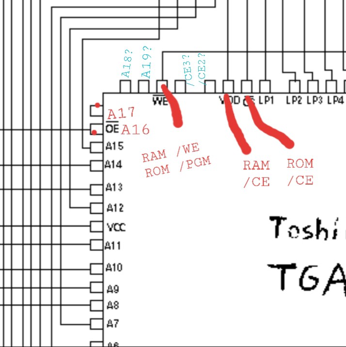
So.... I could do the same, if there's an A18... basically mapping-wise one page would have to be loaded for reading the FLASH, and another page for writing. Of course, I've even bigger plans if there's an A18 (or two more chip-selects)... OR Maybe I could use the ROM's Chip-enable for that... since, of course, writing to the ROM won't actually change its contents... hmmm... (I should probably pop that PGM pin on the ROM, tie it high anyhow, just to be safe).
...
Twenty minutes later... Wait, couldn't I just add some glue? Maybe just an inverter on the /WE pin. Hmmm...
...
Now it gets even weirder...
http://www.datamath.org/Graphing/TI-86_ES.htm
The "Engineering Sample" TI86 has the same FLASH chip I was planning to use... Now, it'd be easy enough to believe they just used them for devel, maybe even popped 'em in and out of a socket to plop in a chip programmer, then had a bunch of those chips left-over to send out the engineering samples.... BUT, the 86 definitely has /PGM wired-up to /WE, which definitely would /not/ make sense to route all the way across the PCB unless they actually intended to use it. But this chip's datasheet makes it perty durn clear /OE has to be high when writing. And I'm perty durn certain it's tied low.
...
AND EVEN WEIRDER:
...Because, yahknow, I didn't spend most an afternoon verifying it was tied low before writing it up.
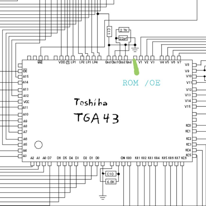
OK... So now we have an /OE on the ROM... which I coulda sworn didn't exist before.
Discussions
Become a Hackaday.io Member
Create an account to leave a comment. Already have an account? Log In.