
In the last post I mentioned you shouldn't change the digits of the nixie tube by changing the cathode. So let's take a look at the anatomy of a tube and one possible method of turning them on/off. A nixie tube has one anode - this is the positive terminal where the 170V comes from. It also has around 10 cathodes, depending on the tubes. By making a complete circuit through the anode and one cathode, you light up that particular digit.
The IN-14 tube has two extra cathodes beyond the digits 0-9, one for the left decimal point and one for the right. Other tubes, like the IN-12a or IN-8, only have the digits cathodes.
There are a number of ways to turn the anode on and off. A common one you will find online (and also the original kit this project started from) is using an NPN transistor and a PNP transistor together. The baldengineer.com site has a really good write up on this, which helped me to understand what's going on here. The takeaway is that this is NOT a Darlington pair - which is what people think two transistors connected like this are. This is using an NPN transistor as a low side switch (meaning the switch, in this case the transistor, is on the low side of the voltage, after the load has used some of the power) to turn on a PNP transistor, which acts as a high side switch, (meaning the switch is on the high side of the voltage, before the load).
The big advantage to using this method is that you can electrically isolate the 5V from the Arduino logic from the 170V the tubes need to light up. Yes, this could be done with MOSFETs, optocouplers, or any of a number of other methods, but the high voltage MPSA42 and MPSA92 transistors I used have a 50MHz frequency, which is >3x faster than the Arduino (16MHz), and the tubes themselves can't really be driven much faster than 10-20kHz or else you get bleed through from previous digits. (Though if you don't care about ghosting, they can be driven REALLY FAST!)
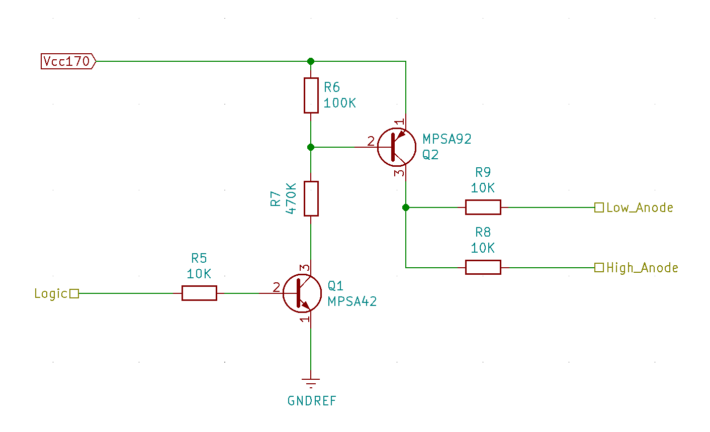
Since I'm turning on each pair of tubes at the same time, there are two anodes being driven by one switch. You could easily have one of these circuits for each tube but I was trying to save output pins. "Logic" is the Arduino digital output, "Low_Anode" is the one's places tube and "High_Anode" is the ten's places tube. Each tube normally uses only 2.5mA, so there is a current limiting resistor before the tube, though with the multiplexing it's a little higher at around 7-13mA.
I looked and looked for some simple formulas to calculate the appropriate values of the resistors, but could not find anything. If you know of a good resource for this please leave a comment below. Ultimately though, I ended up copying the values from the existing circuit because I knew that worked.
Full disclosure: I'm not an electrical engineer. I studied some basic circuits in college but it was only one class and then never touched it again until this project. I copied the circuits I used from what's available online and tried to understand what's happening as best I could. When I first built this circuit, it didn't work, and I spent days troubleshooting it. Finally I realized that the transistor datasheet was garbage and it made it look like the order of the pins was backwards when facing the flat side, at least to my newbie eyes. Once I flipped the transistors around it worked perfectly! I can now turn off the anode before changing digits!
Next up: Cross-fade attempt #1 which resulted in failure.
Discussions
Become a Hackaday.io Member
Create an account to leave a comment. Already have an account? Log In.
As for calculating the anode resistors, the strike voltage of the nixies is around 170V but once turned on the sustaining voltage is more like 150V (exact voltages depend on tube model). So the resistor takes up the difference. With the sample figures 20V across 10k gives 2 mA current, in the ballpark, as you say there.
Are you sure? yes | no
Your PNP transistor has the emitter and collector swapped in the schematic (but is probably wired up correctly in-circuit). You can tell from the emitter arrow which indicates the direction of current flow.
Are you sure? yes | no
Well dang! You have a great eye, thanks! Yes, the bread board is wired correctly, BUT... the board layout in kicad was wrong as a result of that. So glad you caught that before I sent off the board to get made! I've updated the schematic in the post.
Also, this was not the reason I spent all the time troubleshooting it - I had both the NPN & the PNP transistors backwards in the actual circuit on the breadboard. I'm not sure when I introduced the error in the schematic, as the source schematic I was using did not have this error.
Are you sure? yes | no