0%
0%
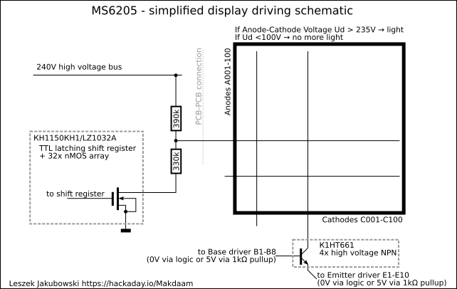
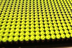
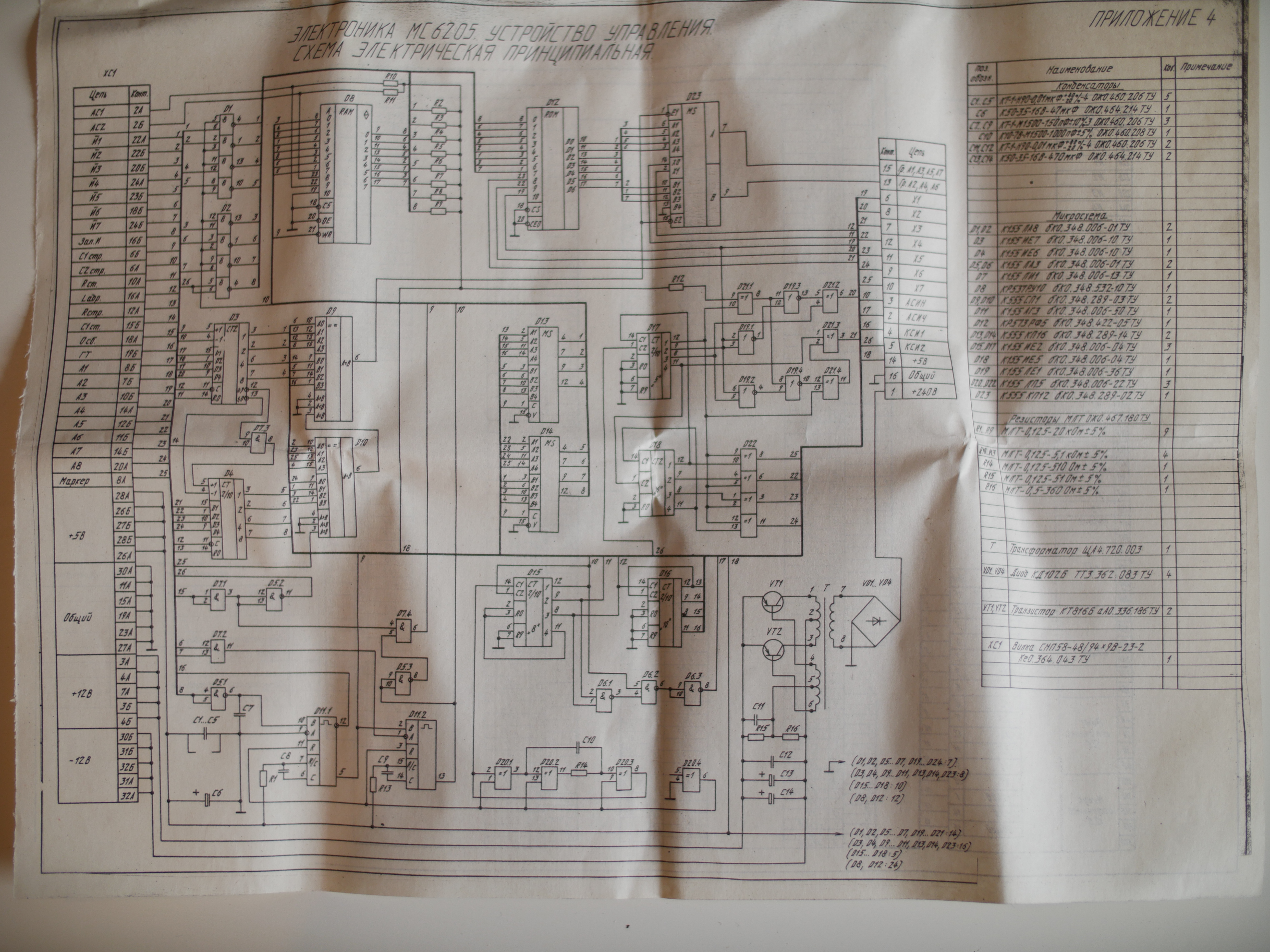
MS6205 graphical mode
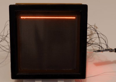
Modifying the MS6205 (МС6205) display to control every pixel individually instead of sending text characters
 Leszek Jakubowski
Become a Hackaday.io member
Already have an account? Log in.
Just one more thing
To make the experience fit your profile, pick a username and tell us what interests you.
Pick an awesome username
hackaday.io/
Your profile's URL: hackaday.io/username. Max 25 alphanumeric characters.
Pick a few interests
Projects that share your interests
People that share your interests


 Frederic L
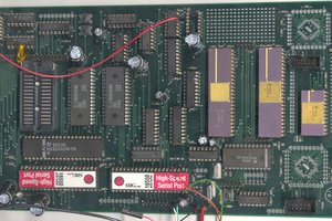
 Keith
Keith
 Stephen G
 twl
twl