 Leszek Jakubowski
Edit: I had KSI1 and KSI2 mixed up. I fixed the pin and graph descriptions.
After connecting an oscilloscope to the different pins of the logic PCB-anode PCB interface I think I've got enough info to work on driving every connected pixel.
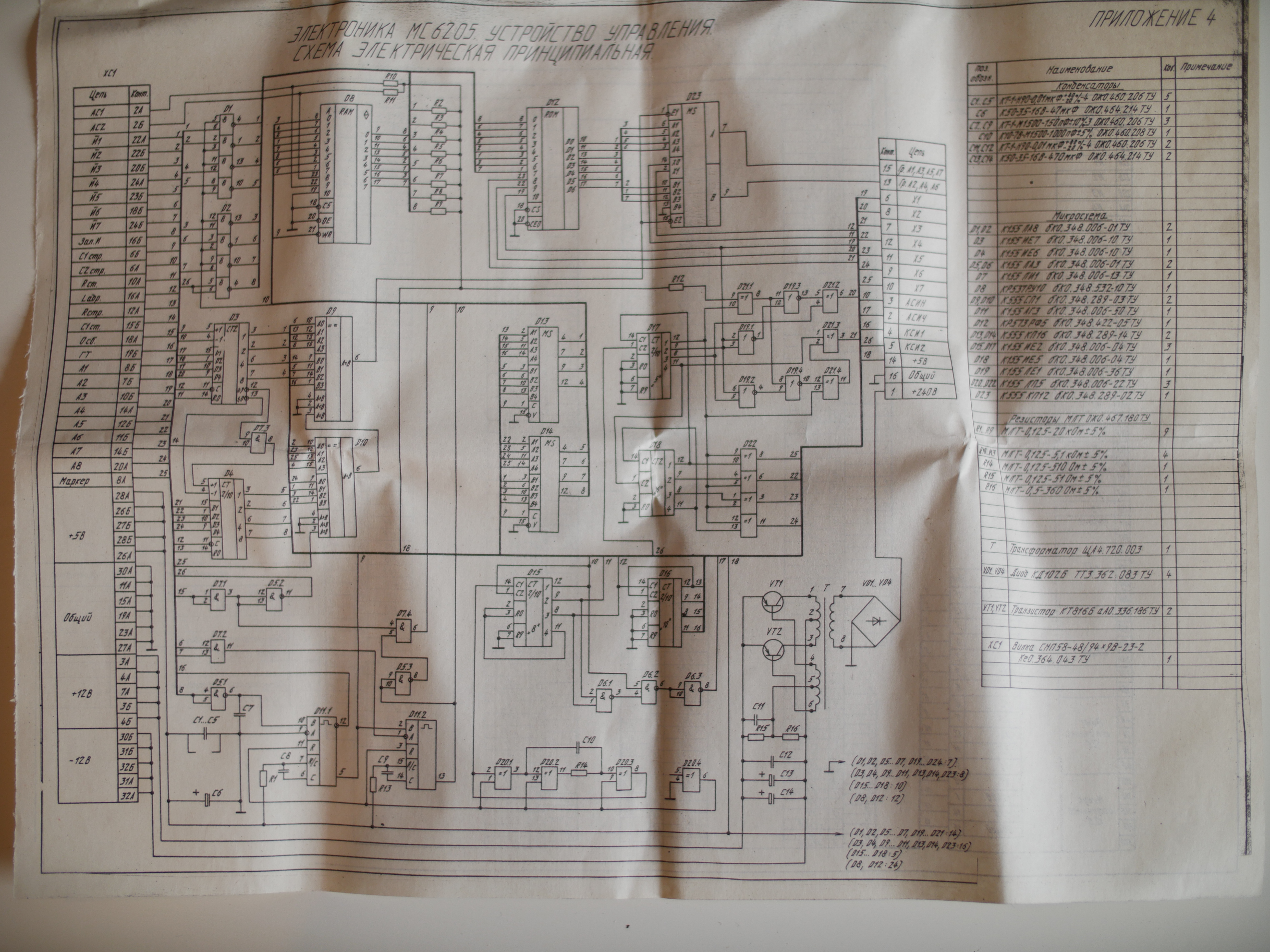
The pins are as follows:
- +240В (+240V)
- АСИЧ (ASICh) - anode clock 2 (for even anodes)
- АСИН (ASIN) - anode clock 1 (for odd anodes)
- КСИ2 (KSI2) - cathode clock 2 (only signal going from anode driver PCB to logic driver PCB)
- КСИ1 (KSI1) - cathode clock 1
- Х1 (H1) - lowest bit of cathode selection number
- Х3
- Х2
- Х6
- Х7 (H7) - highest bit of cathode selection number
- Х5
- Х4
- Гр. А2, А4, А6 (Gr. A2, A4, A6) - even anodes serial data
- +5В (+5V)
- Гр. А1, А3, А5, А7 (Gr. A1, A3, A5, A7) - odd anodes serial data
- Общий - Ground
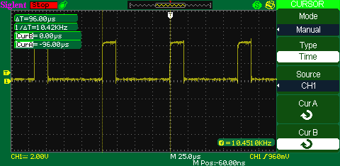
The clocks for loading anode data work at a 3:4 ratio since every character is 7 lines high and there are 4 odd and 3 even pixels to load. The loading is split to speed up the whole process.
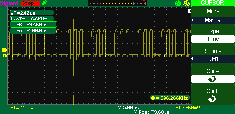

The clocks are going at about 416kHz, but the exact timing is not critical. The clock source is a RC stabilized oscillator done on 4 XOR gates of D20 (bottom of logical board schematic. As long as the shift registers, RAM, ROM and address generation logic can keep up the clock signal is valid.
Next up is the Cathode clock pulses by the monostable trigger on the anode driver side from a square wave into very short pulses. It's sent back to the logic board on KSI2 (cathode clock 2) as a "ready for another vertical line" signal. This is the only signal going backwards.
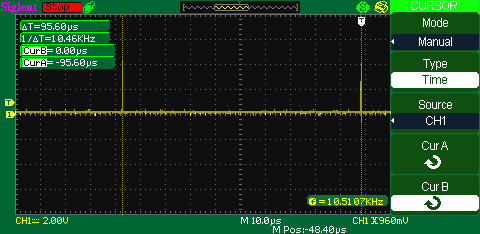
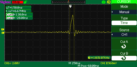
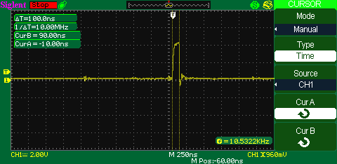
The square pulse, which is sent after all the Anode data is shifted into the registers and the right number is set on H1-H7 to select the loaded vertical line and latch the data from the anode shift registers into outputs. Triggers latch on falling edge. It's just a square blip on KSI1 (cathode clock 1).

KSI2 and ¬KSI2 are more interesting on the anode driver PCB, where they control the latching of both the H1-H7 cathode selection number and the anode shift registers into the actual high voltage outputs.
Discussions
Become a Hackaday.io Member
Create an account to leave a comment. Already have an account? Log In.