 AVR
AVRHey so I got a little ambitious over the last few days and did a lot of work to the PCB. I'm happy to share my first pass on routing on both PCBs for this project log. First off there were a number of changes to the schematic and the connectors used on the board, these specs are still subject to change over the course of the project. Anyways I swapped out the fancy SMT connectors for 2.54mm pitch pin header and broke out all the signals to a single header. This header allows the radio to communicate over SPI or USART, the header also allows for power to be fed into the board for applications where USB power is unavailable. I also swtiched to this kind of connector because its more popular and easier to interface with, 2.54mm Pitch is pretty standard.
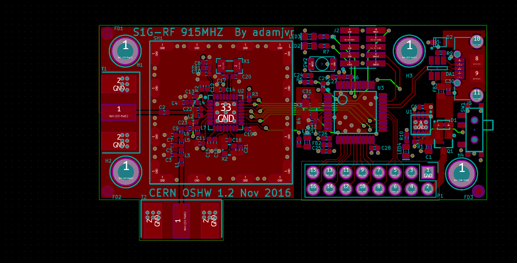
So this project encompasses two versions of the same radio circuitry, one version with separate PA/LNA matching circuitry and antennas, the other one uses a combined match and a single antenna. The combined implementation is meant for application where size is an issue, the separate implementation is for size independent applications such as drone ground stations.
Before I unveil the PCBs, I wanna outline the general function of them, I didn't elaborate on that all that much in the first post. There is a diagram below to help understand:
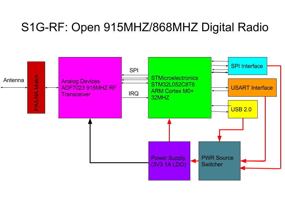
The diagram above shows the general system overview of both of the S1GRF PCBs. The heart of both is the ADF7023 transceiver IC, this is controlled by an ARM Cortex M0+ over SPI serial. The ARM Cortex M0+ being used is the STM32L052C8T6 its a simple ARM micro-controller clocked at 32MHZ. The STM32's job is to provide a USB 2.0 interface, USART, and SPI interface for connecting to user applications. How these interfaces will function will be later defined when the firmware gets developed. Also the serial interfaces that are available on the pin connector along with GPIO pins. Also in the diagram is a power source switcher, this is essentially a simple circuit consisting of a MOSFET and diode, this switches the LDO to be fed off the USB port instead of the pin connector.
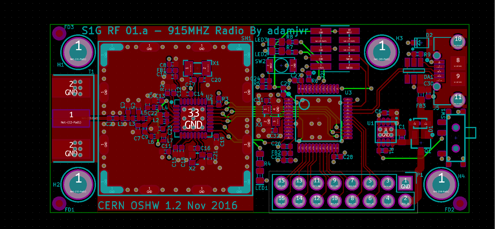
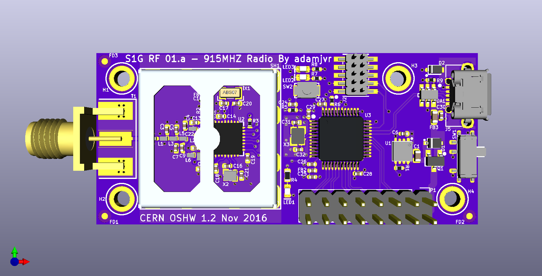
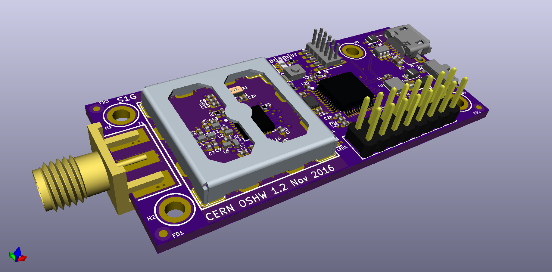
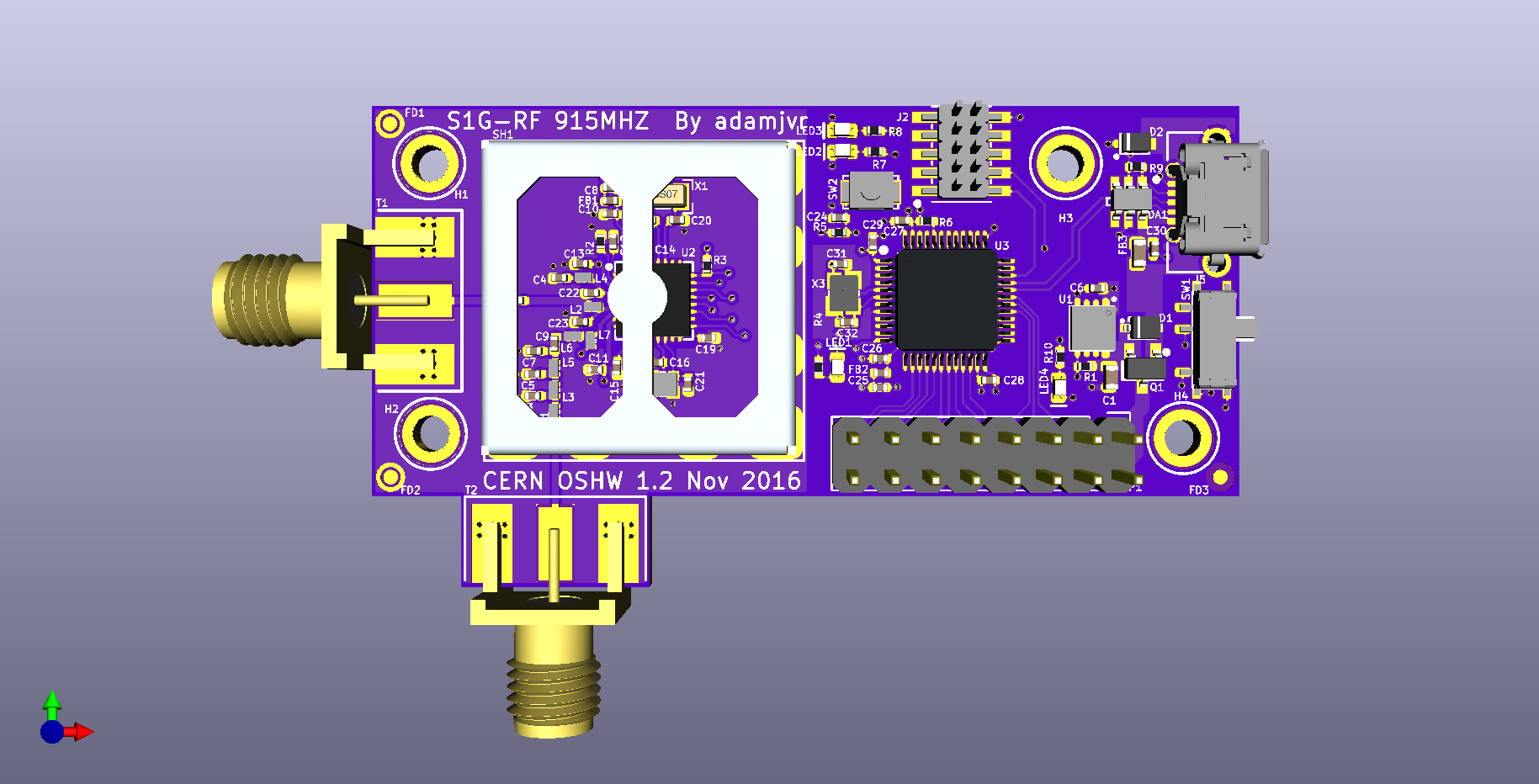
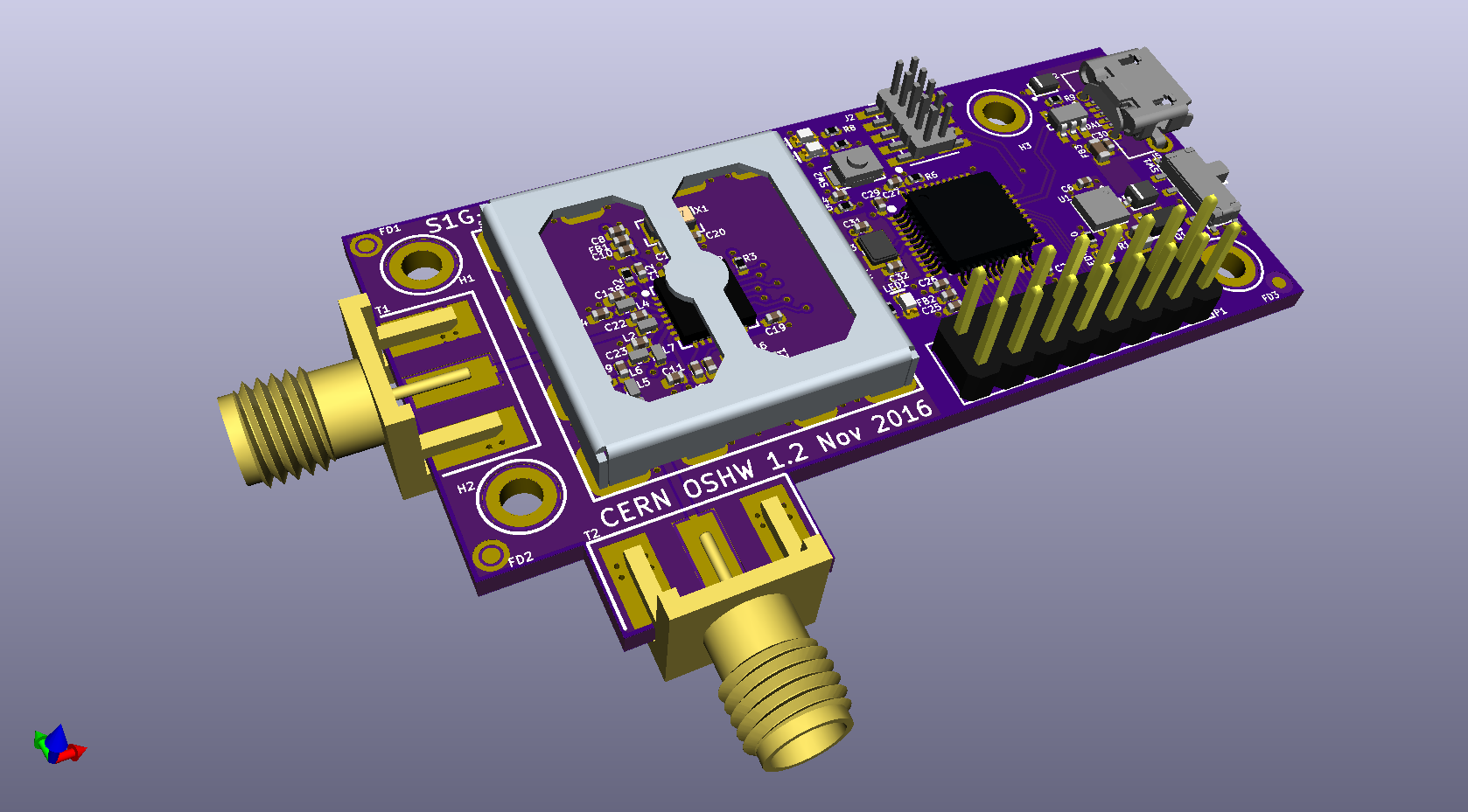
Now for the PCBs! First here is the combined PA/LNA match implementation:
2D From KiCAD:
KiCAD 3D Top Side:
KiCAD 3D Angled:
Separate PA/LNA Match Implementation:
2D From KiCAD:
KiCAD 3D Top Side:
Discussions
Become a Hackaday.io Member
Create an account to leave a comment. Already have an account? Log In.