 zaphod
Table of Contents:
the project logs are in reverse chronological order and a little annoying to navigate through so here's an index of all of the links:
- Ancient History - explains how this project started and what the goals are
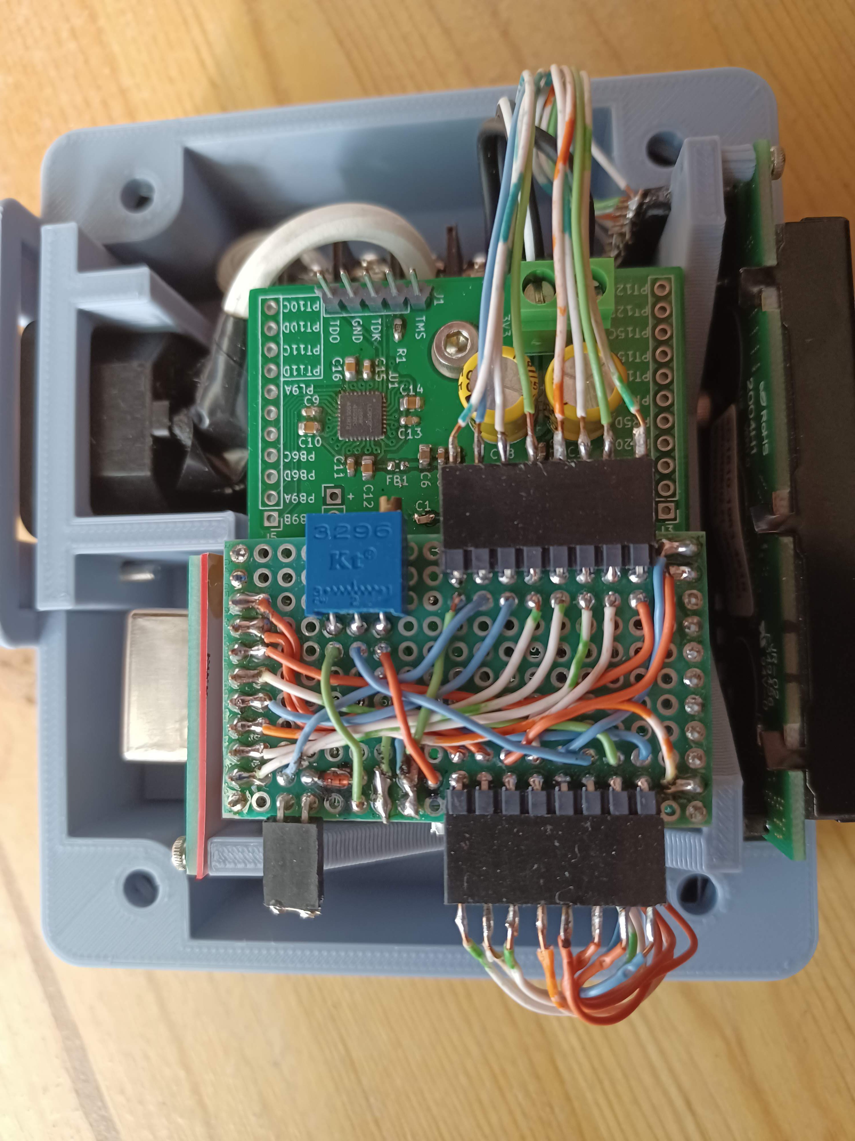
- Version 1 Hardware Circa 2019 - shows off the first iteration of the project
- 2020 V2 and the Current State of the Hardware - ill fated v2, and beginnings of v3
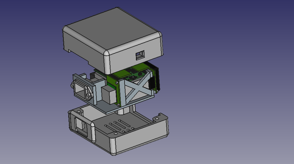
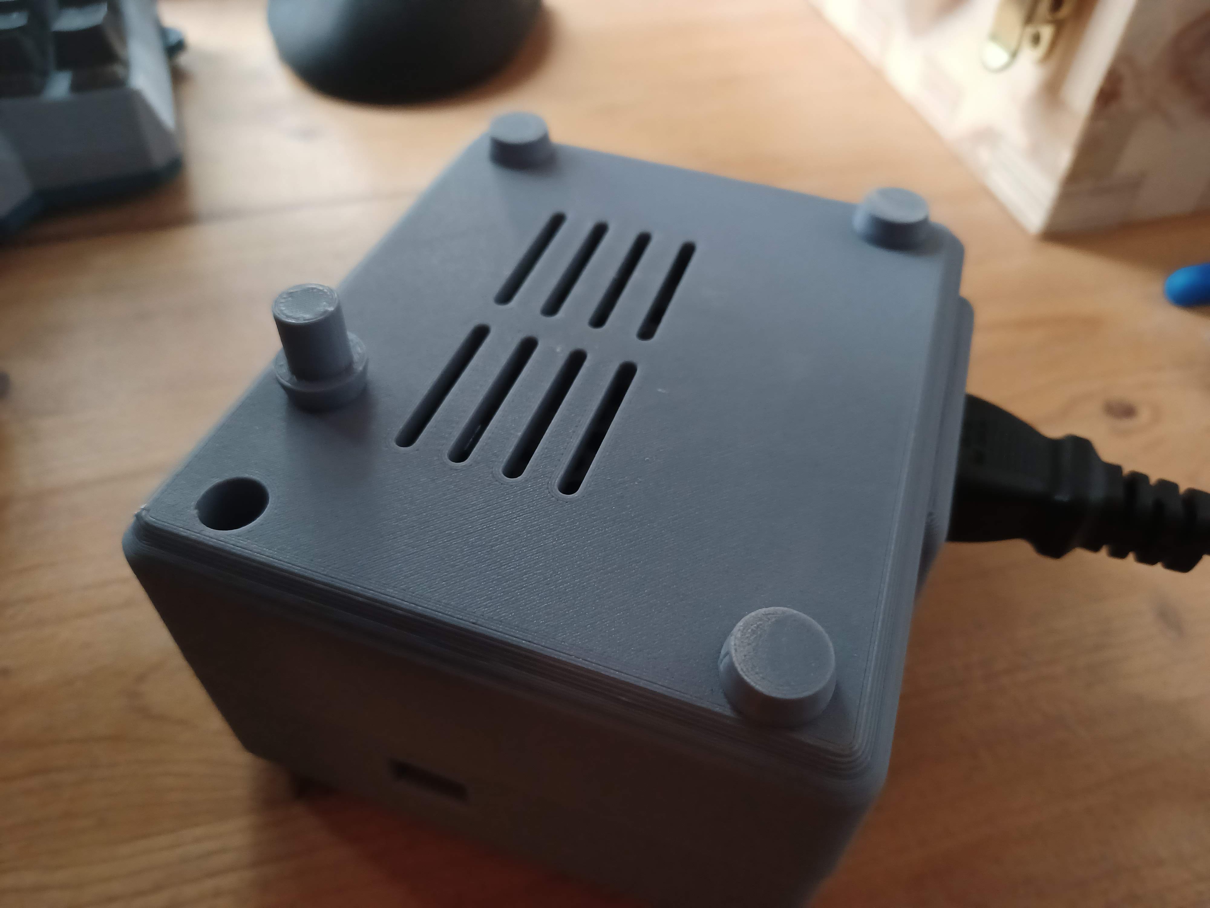
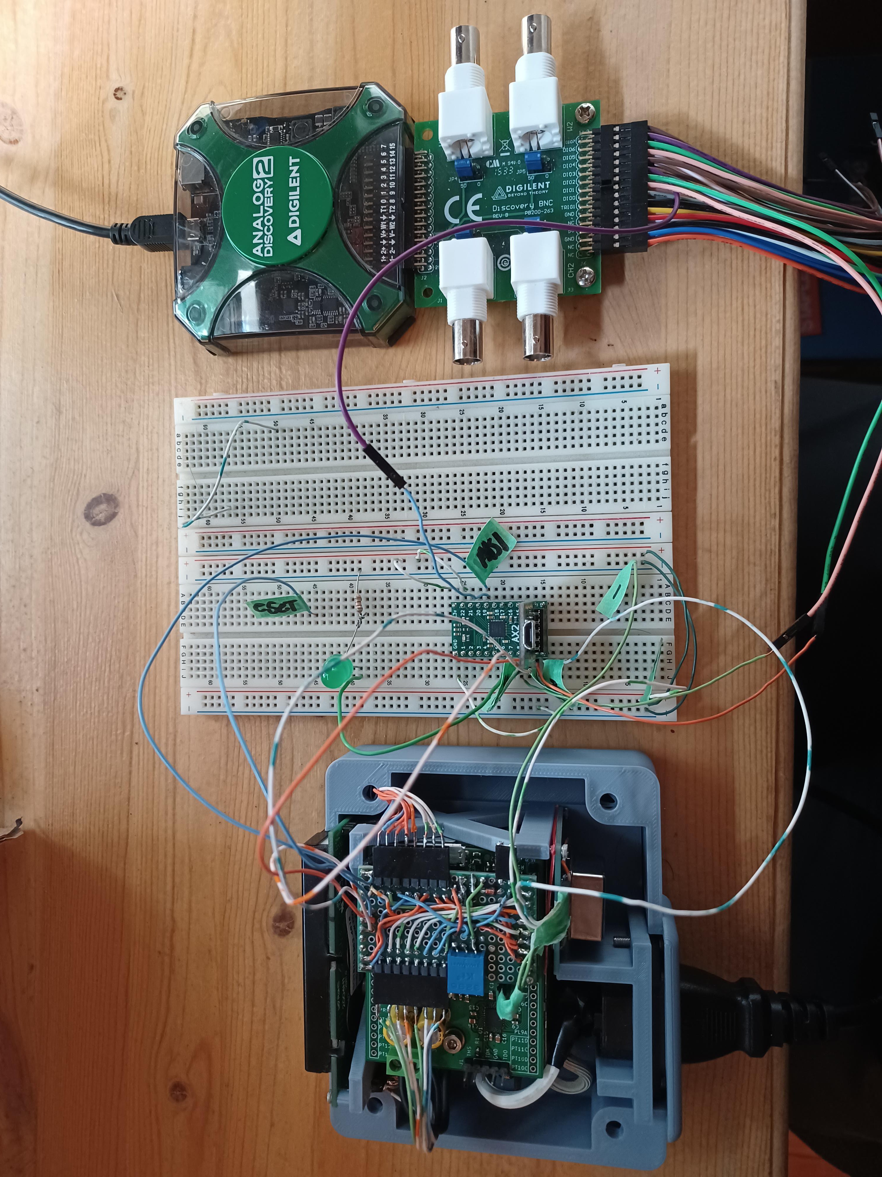
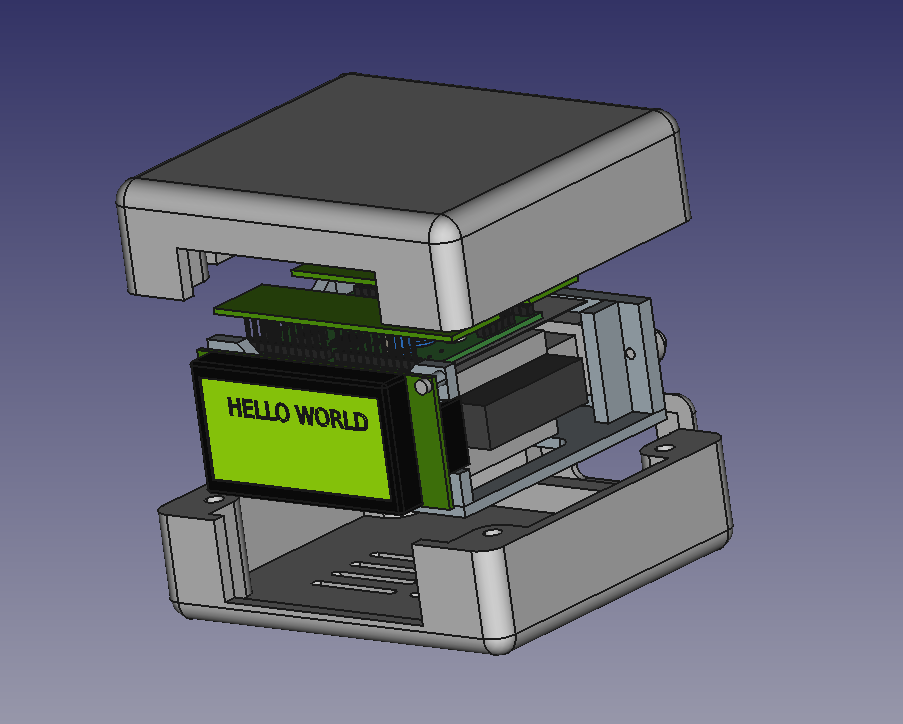
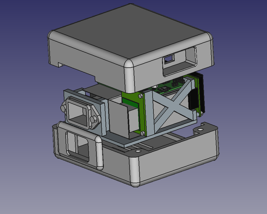
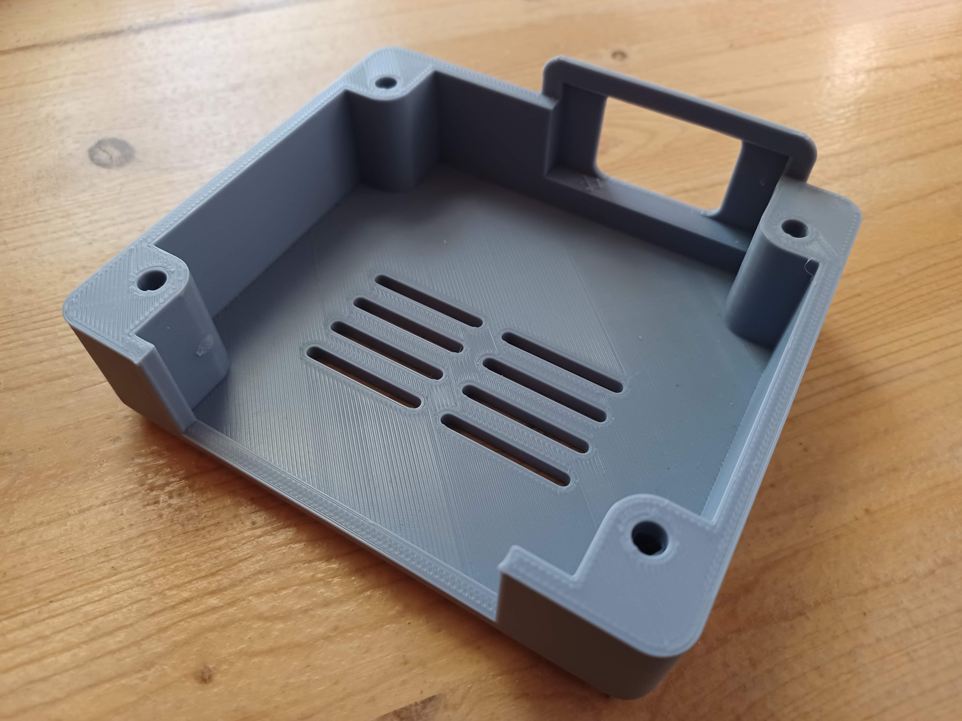
- The 3D Printed Case - the basic mechanical design of the clock
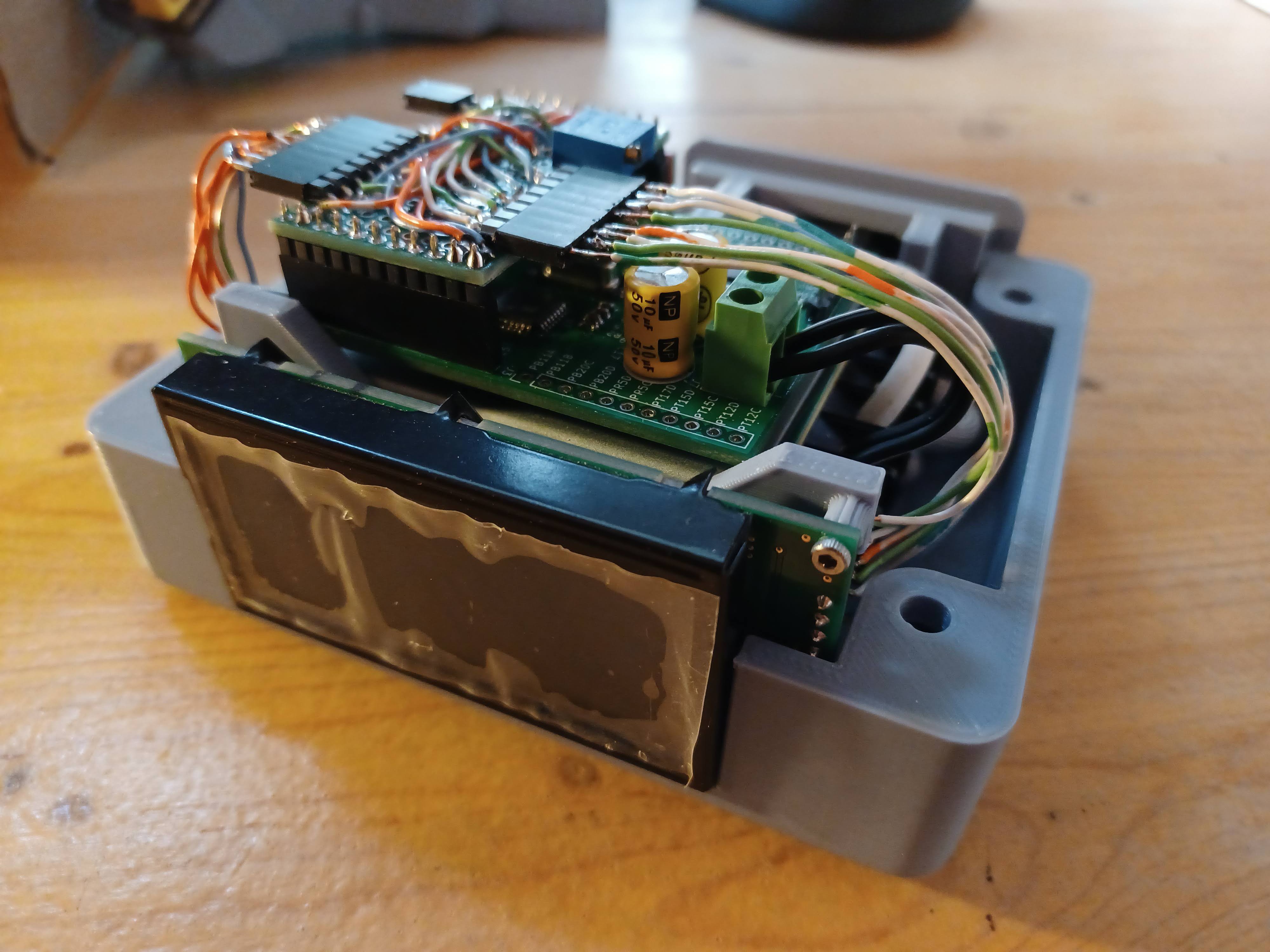
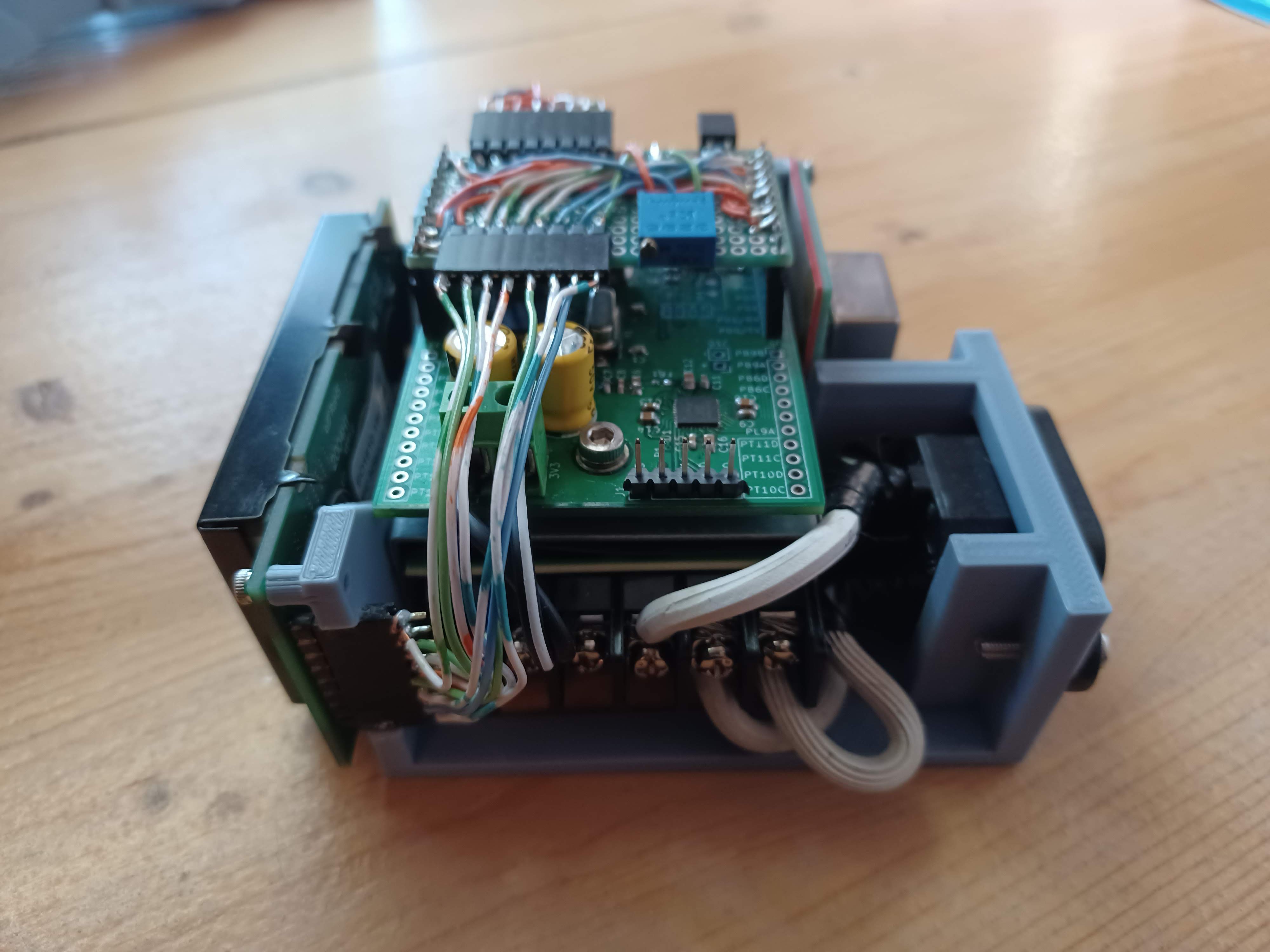
- The Display Interconnect Board - self explanatory
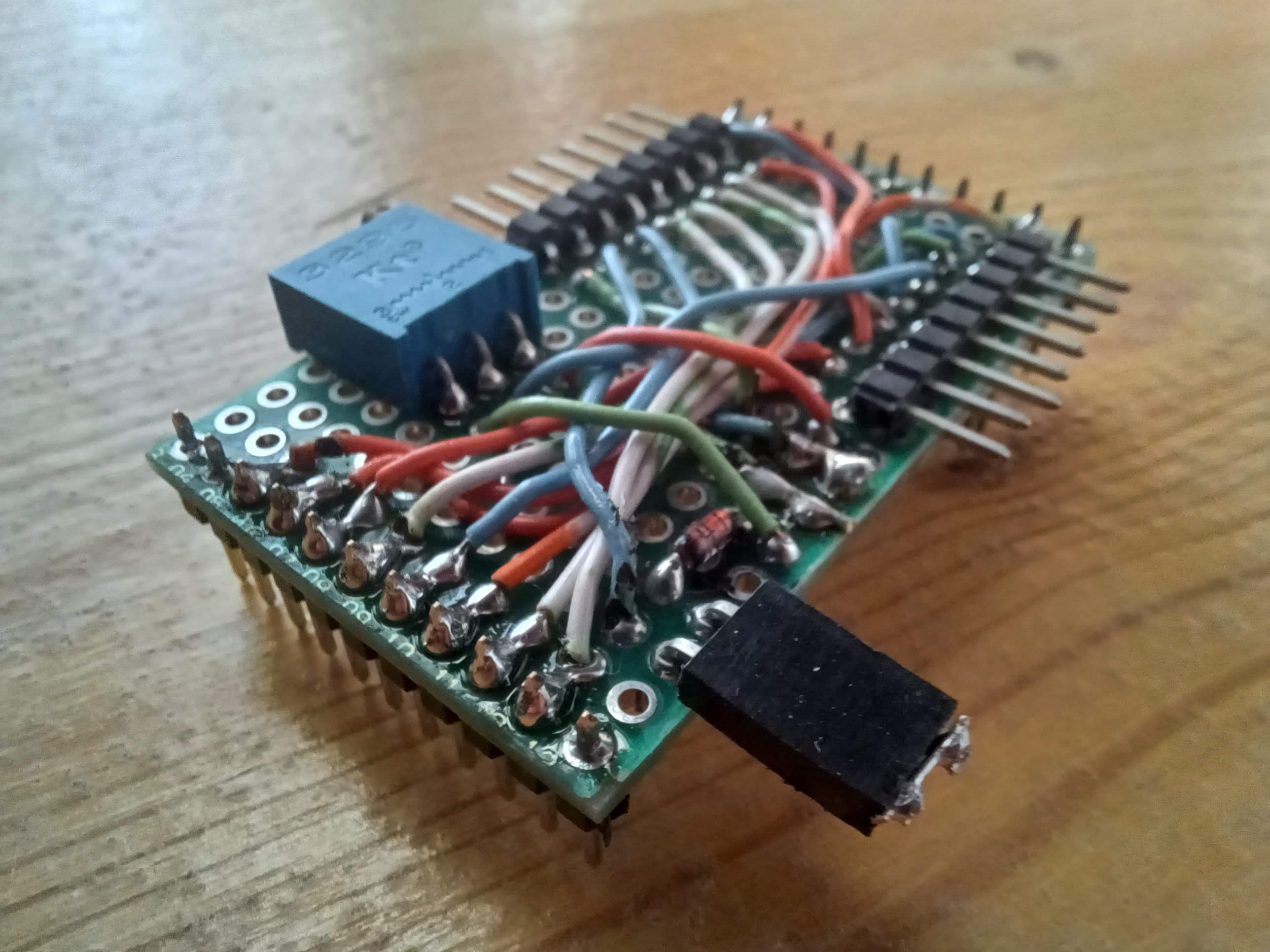
- It Ticks! (Sort of) - I work around some bugs in the v3 board, and get it ticking
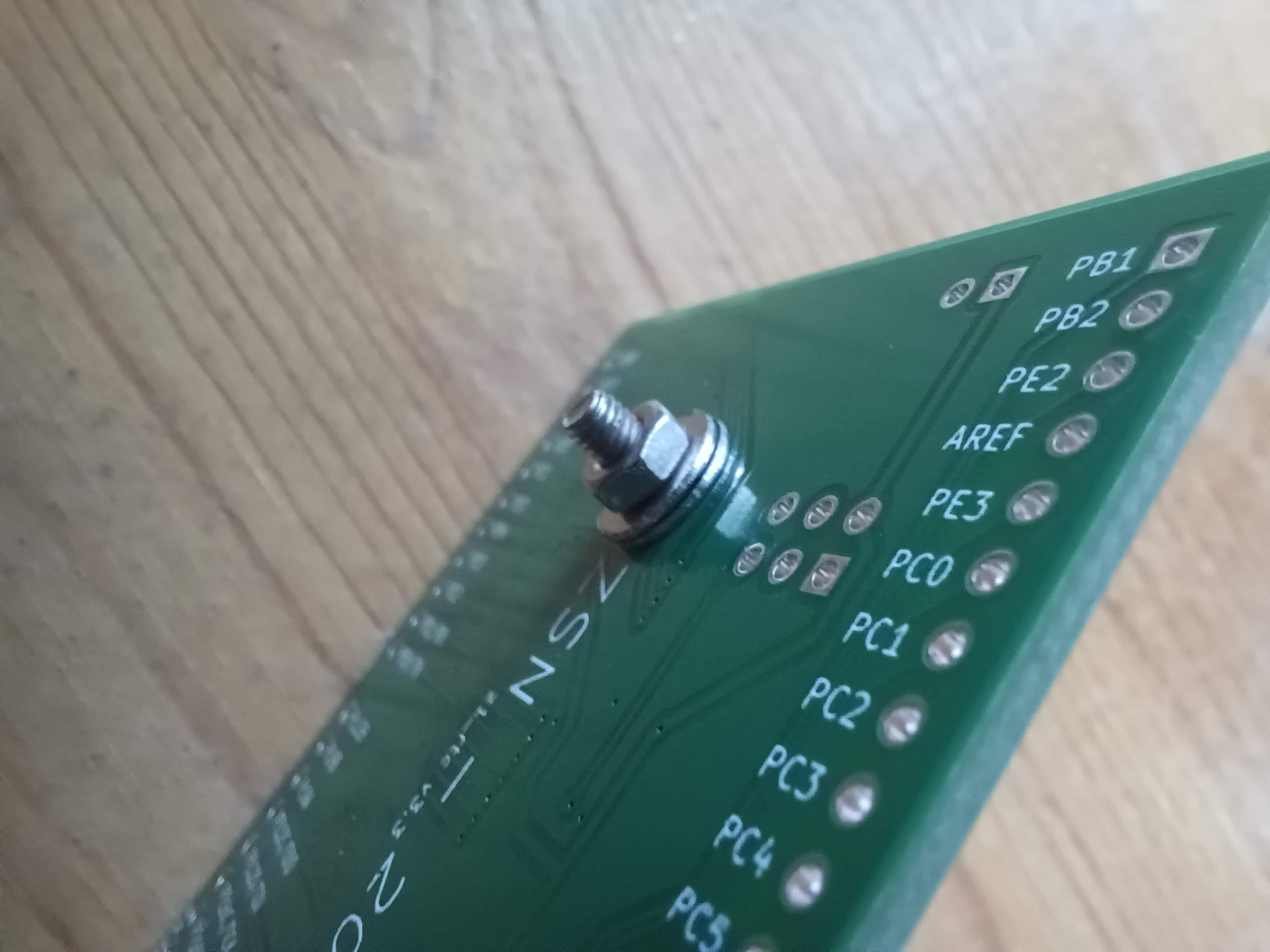
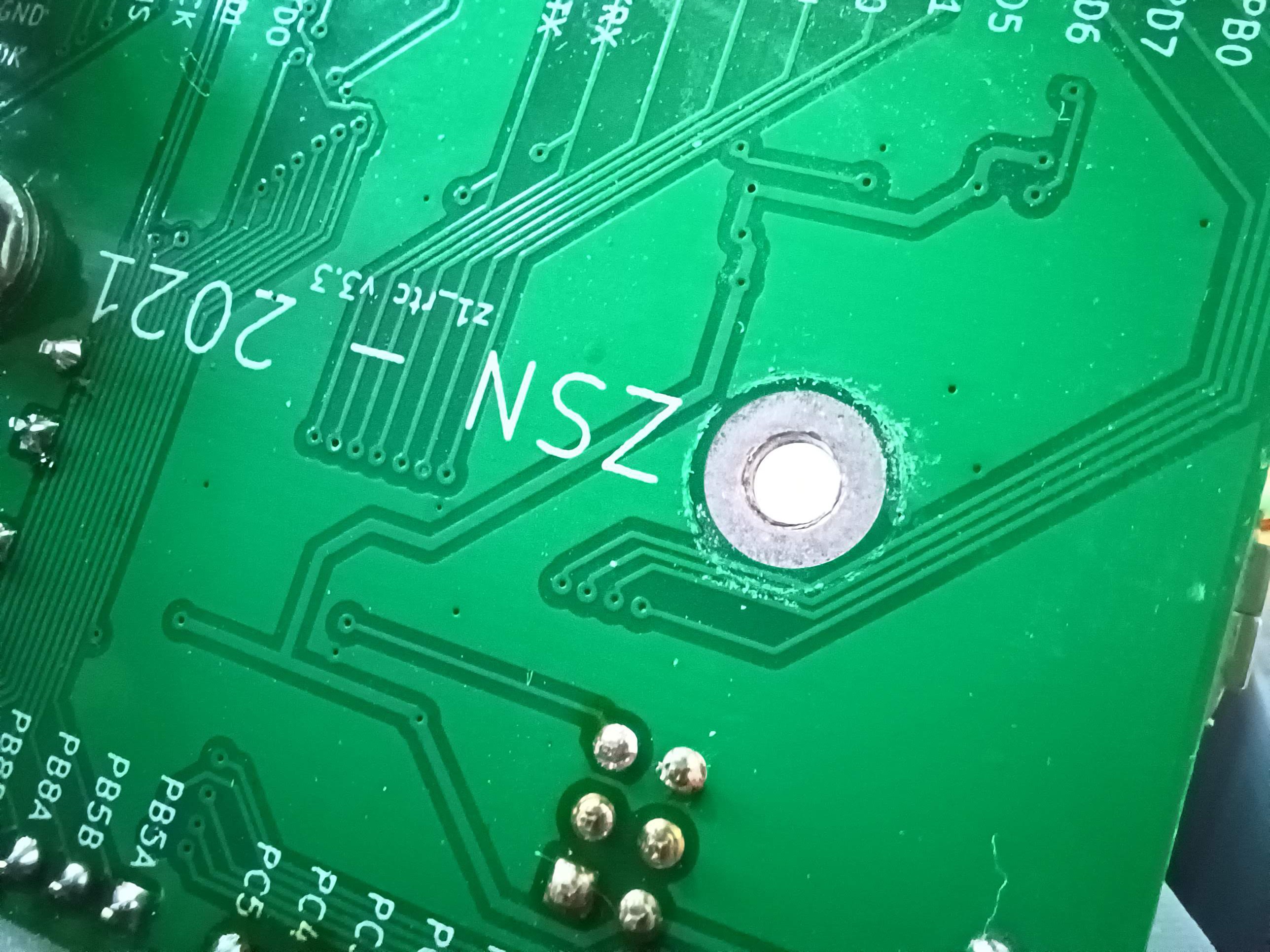
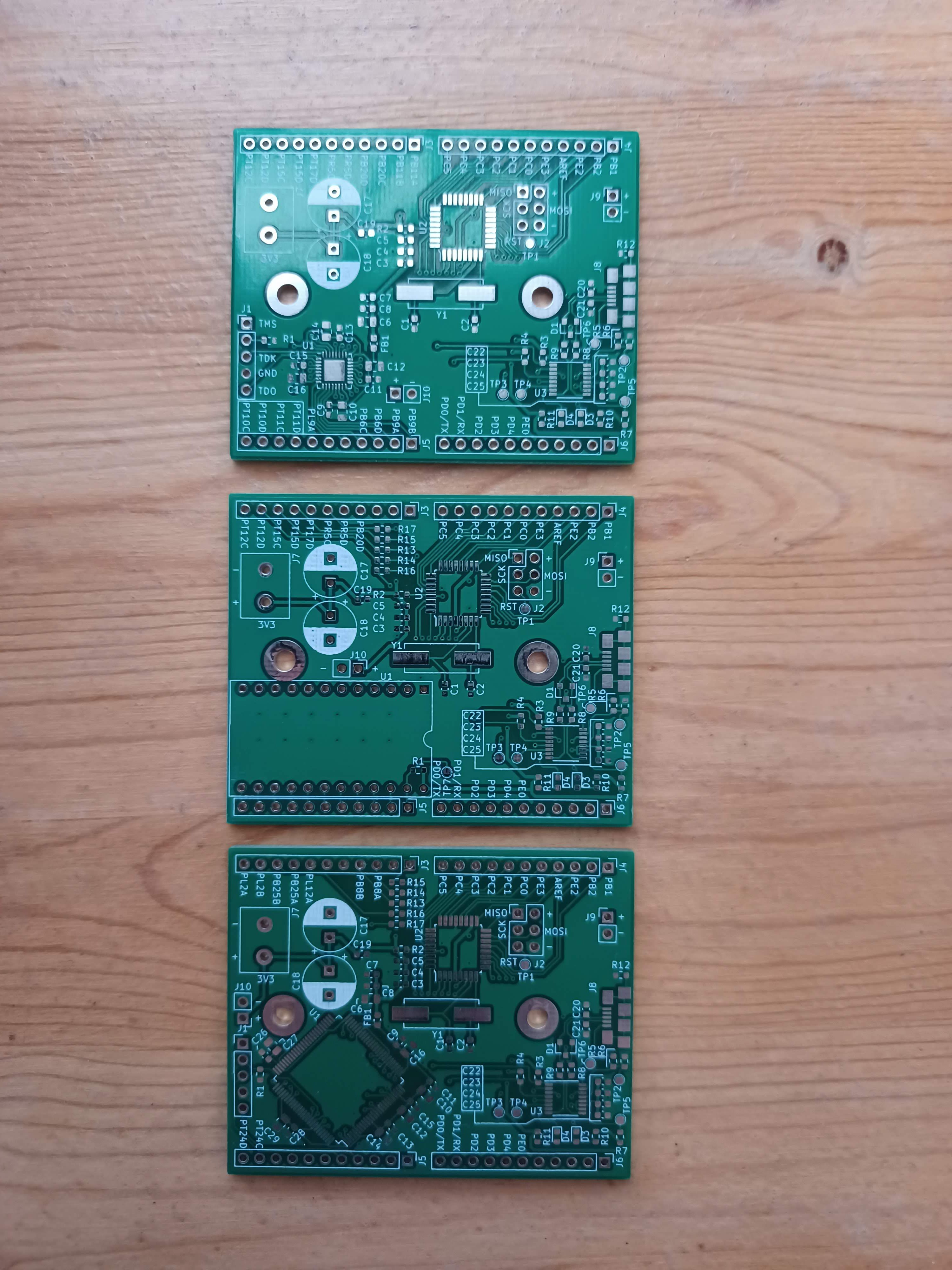
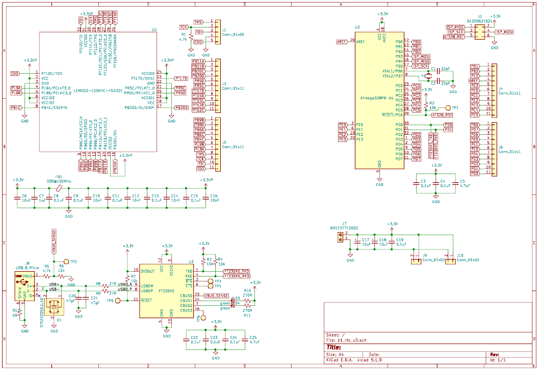
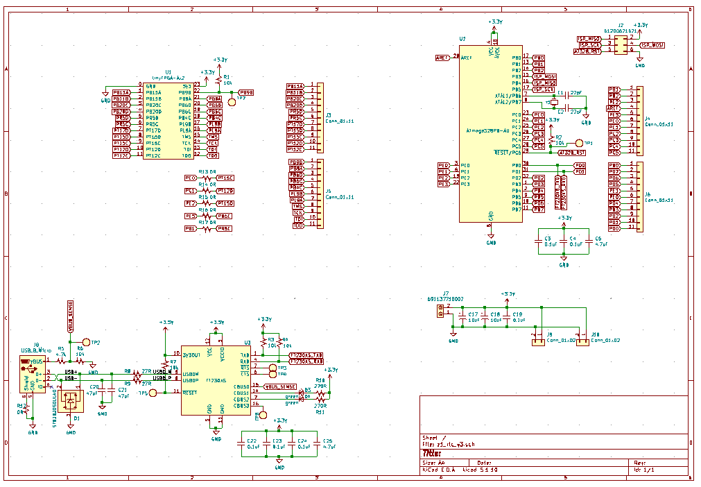
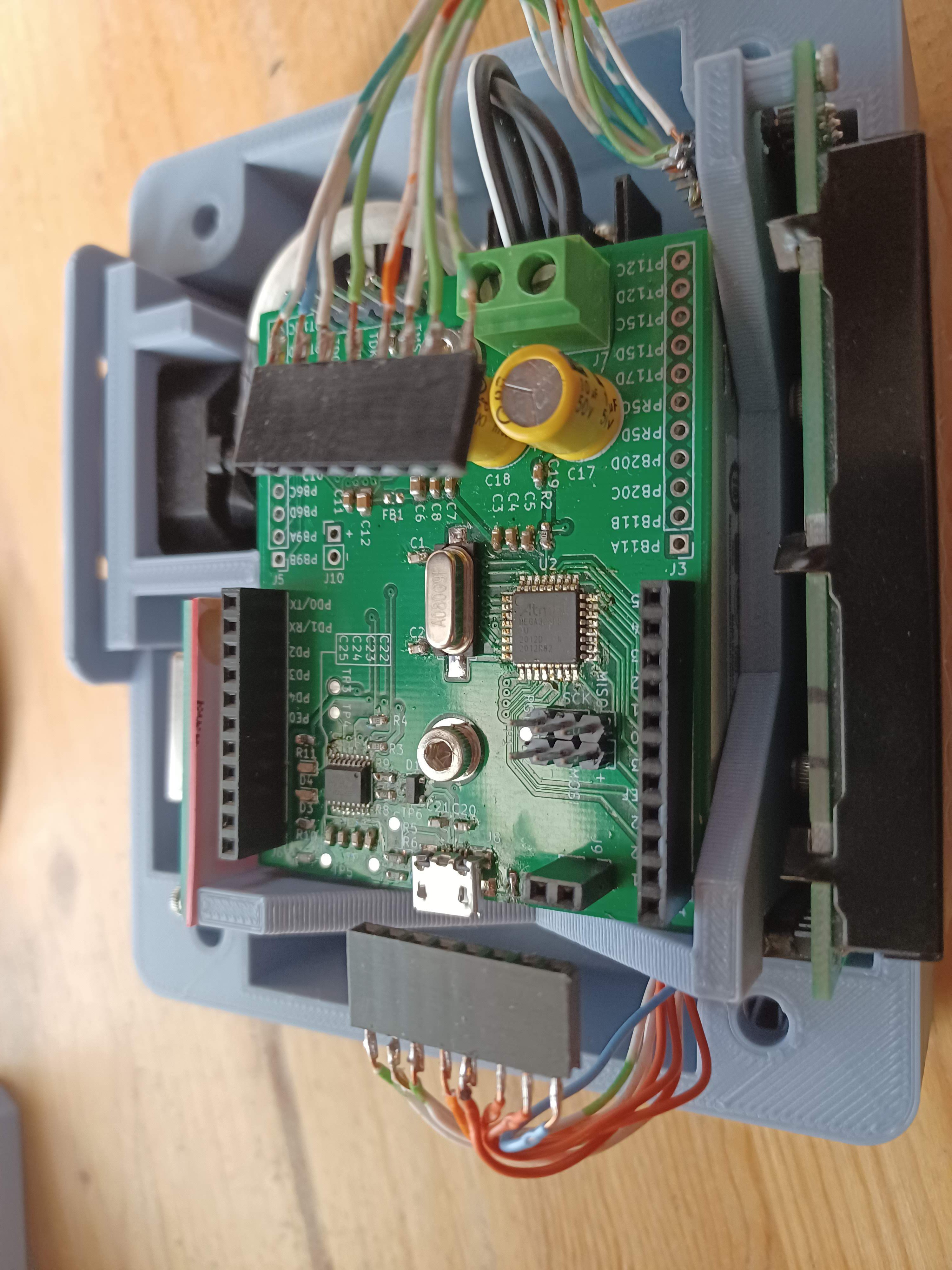
- New PCB Versions - I discuss the v3.2 and v3.3 designs
- It Ticks! For Real This Time - v3.3 bring up
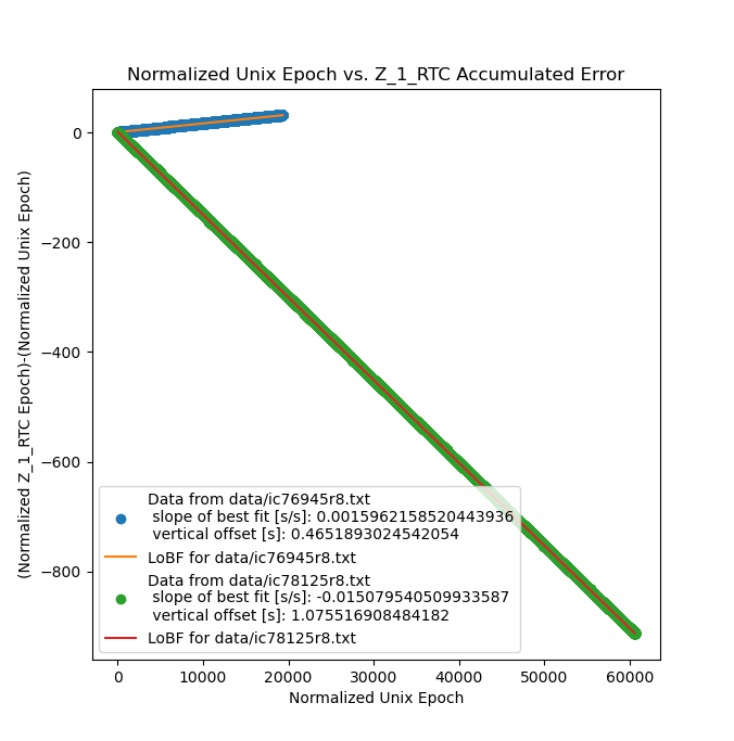
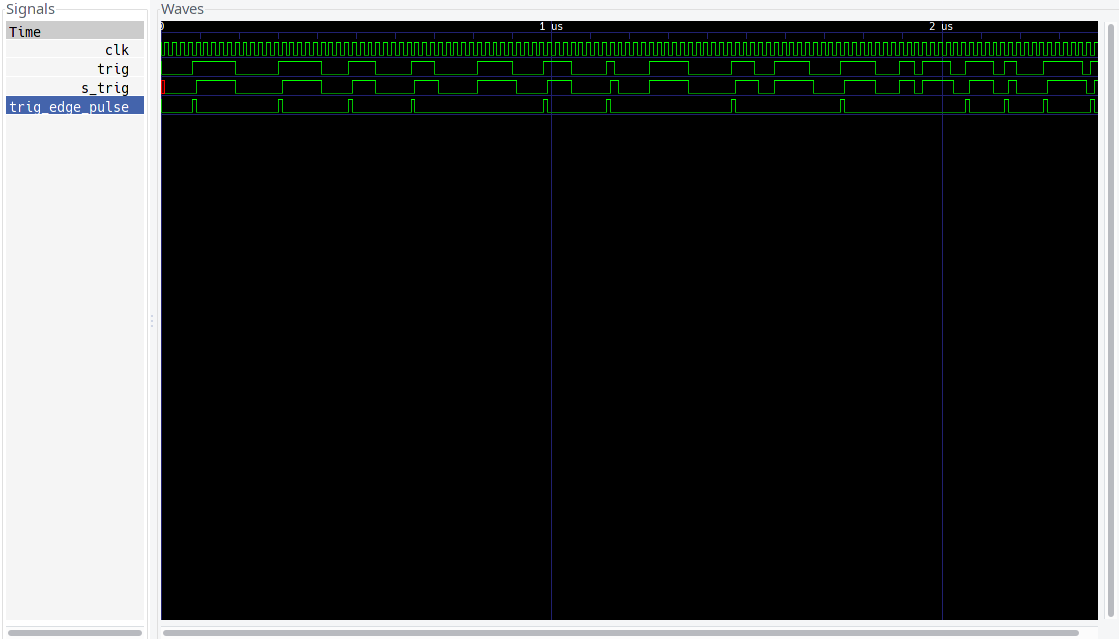
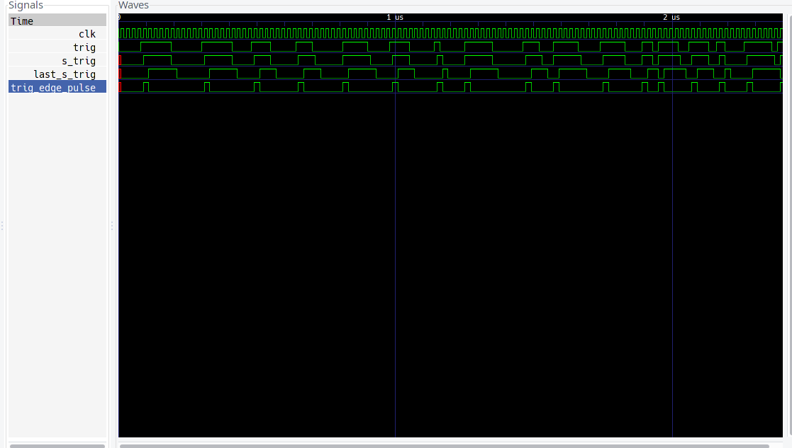
- Ticking Accurately - find and fix verilog bug that was impacting accuracy
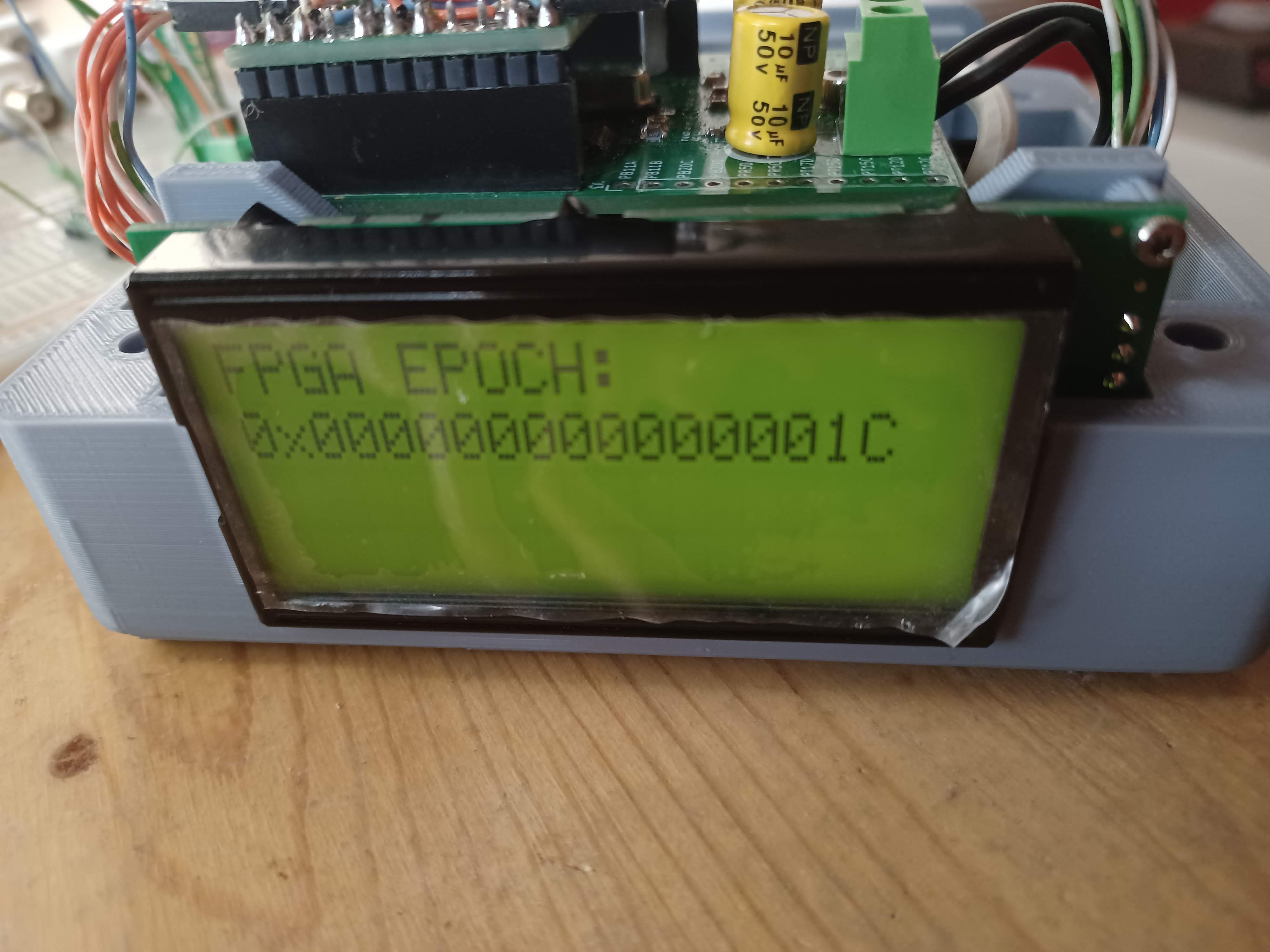
- It Lives! - software/firmware/hardware all work together for the first time
- Squashing Hardware Bugs - fixing integration issues
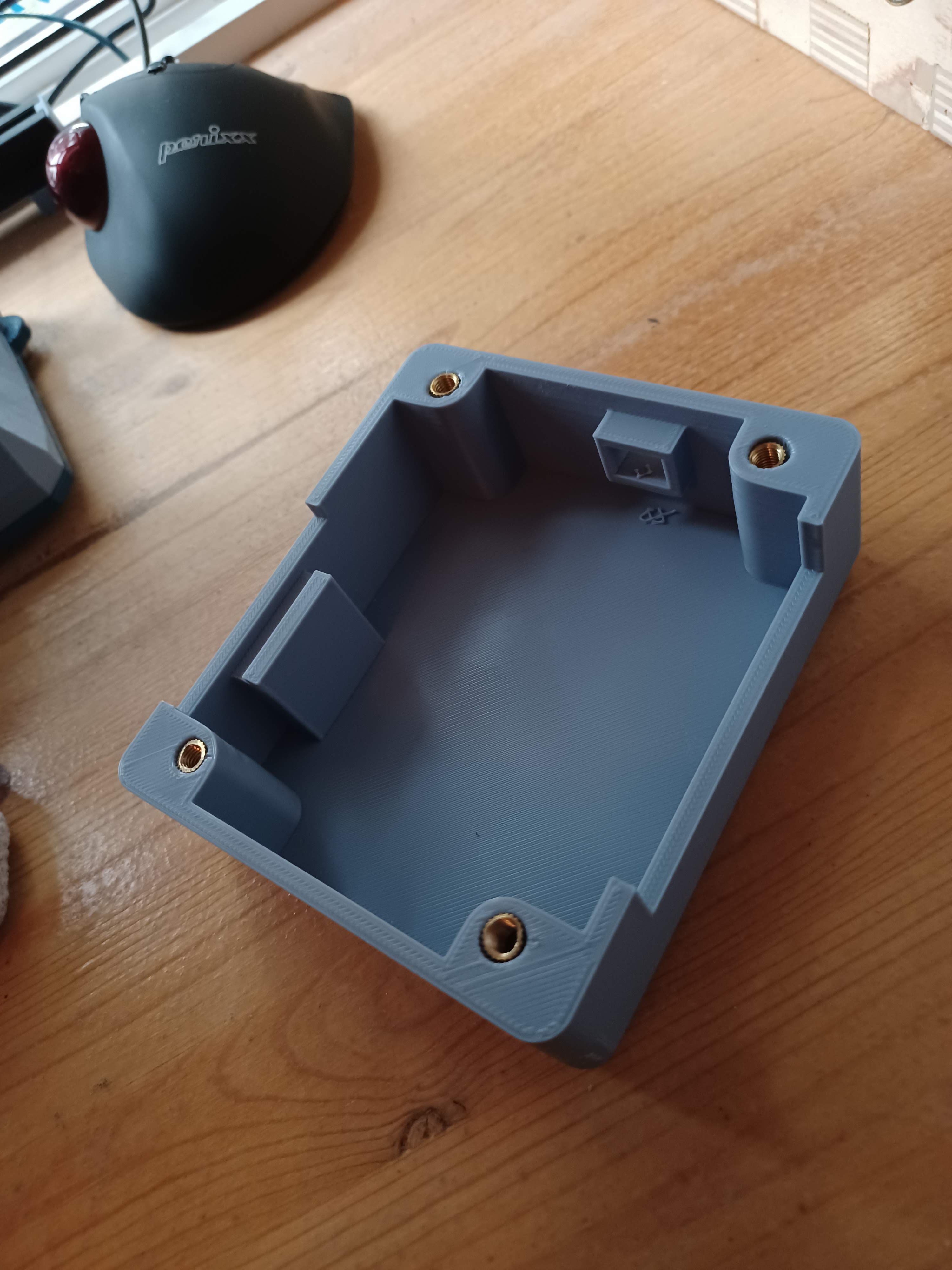
- Updated Case - I redesign the case to fit the electronics
- Conclusion and Next Steps - self explanatory
Introduction:
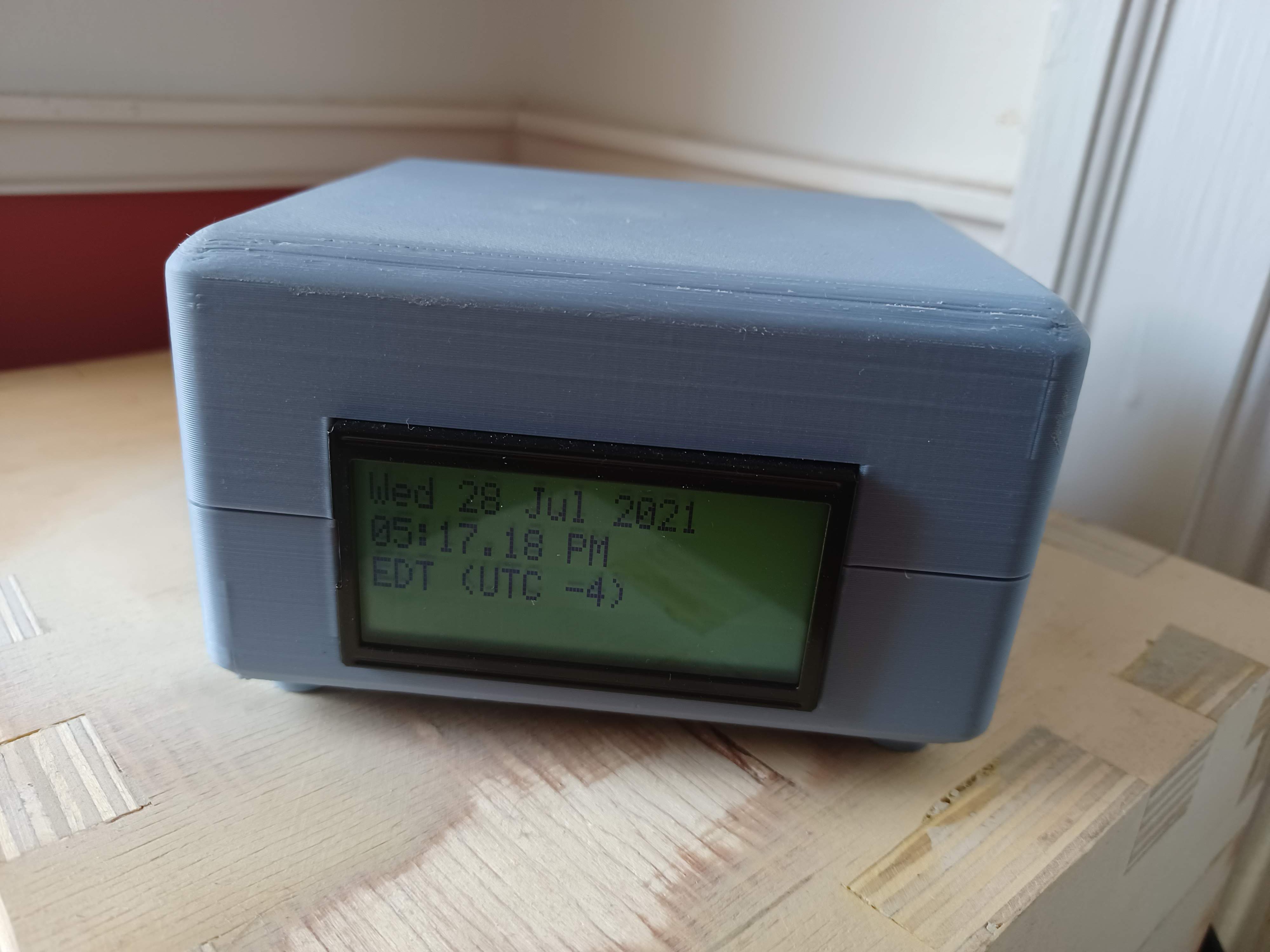
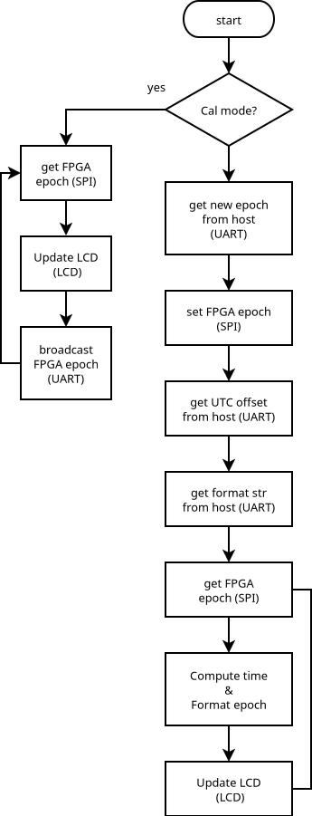
This project is an attempt to build a free running digital real time clock with an accuracy of better than +/- 30 sec/mo (the accuracy of a Casio F91W watch).
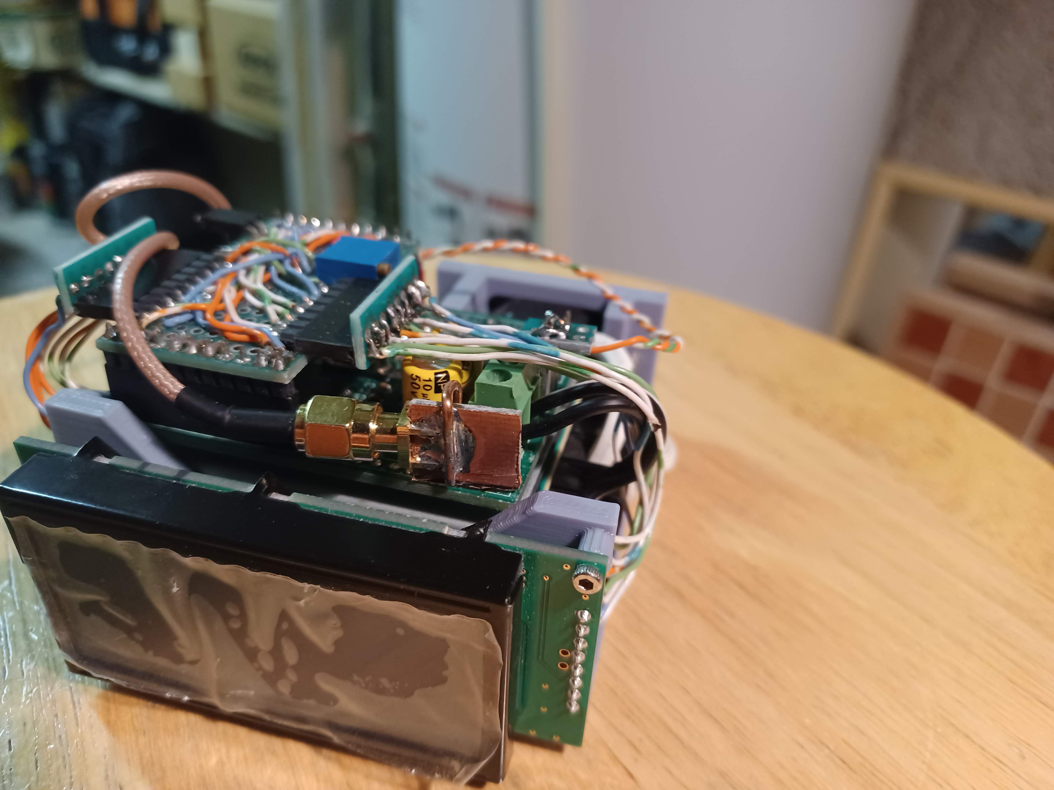
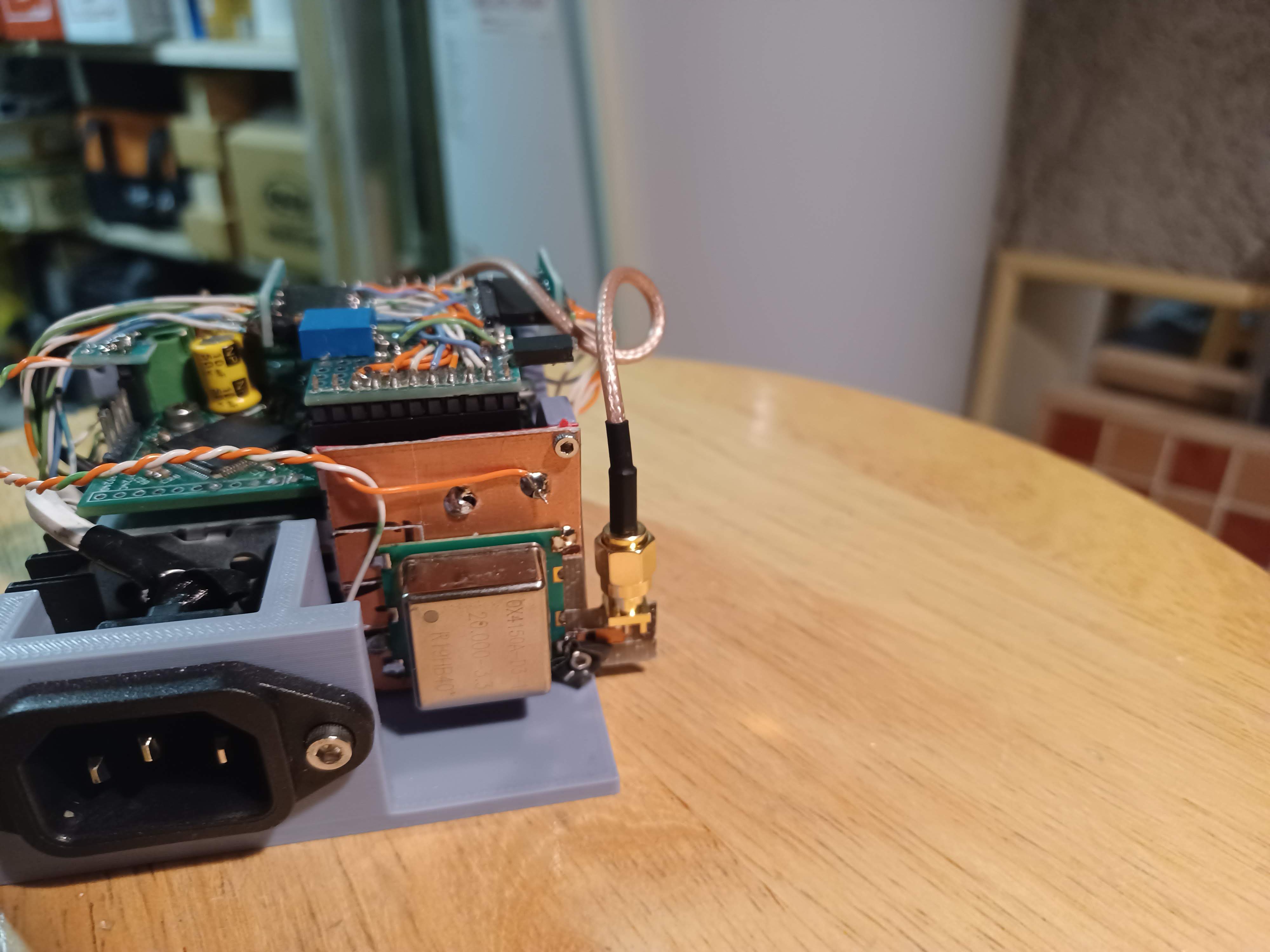
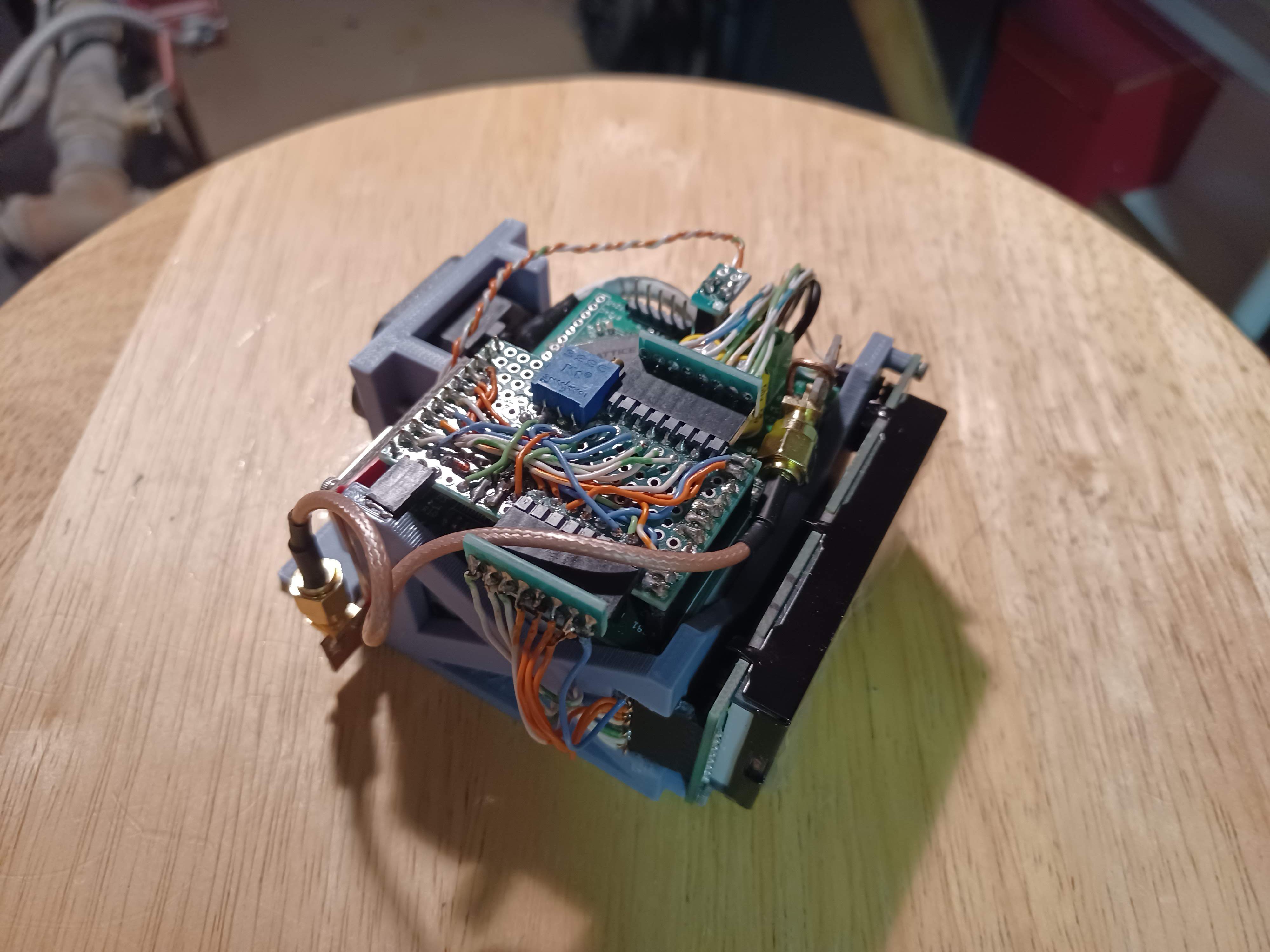
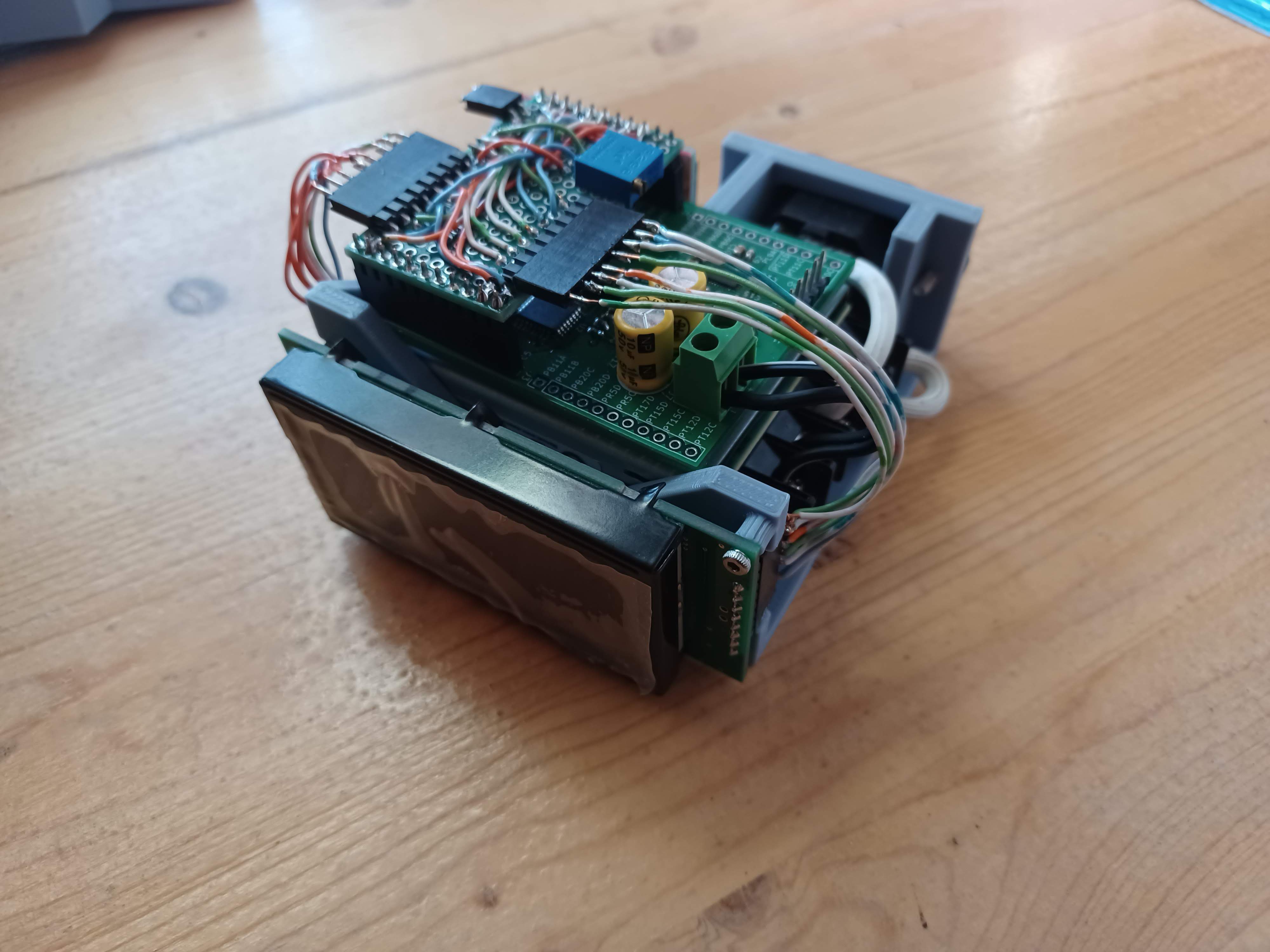
Over the course of the project I design and bring up multiple custom PCBs, write verilog, C, and Python, as well as doing some 3D printing. In the end I was able to get everything working properly (after lots of debugging), and now I have a very accurate little clock that sits on my desk. (not sure exactly how accurate, see project log 13 above, but certainly better than 1 sec/day).
all of the design files for the clock are on my github:
- https://github.com/ZakSN/z_1_rtc
- https://github.com/ZakSN/z_1_rtc_pcb
- https://github.com/ZakSN/z_1_rtc_mech
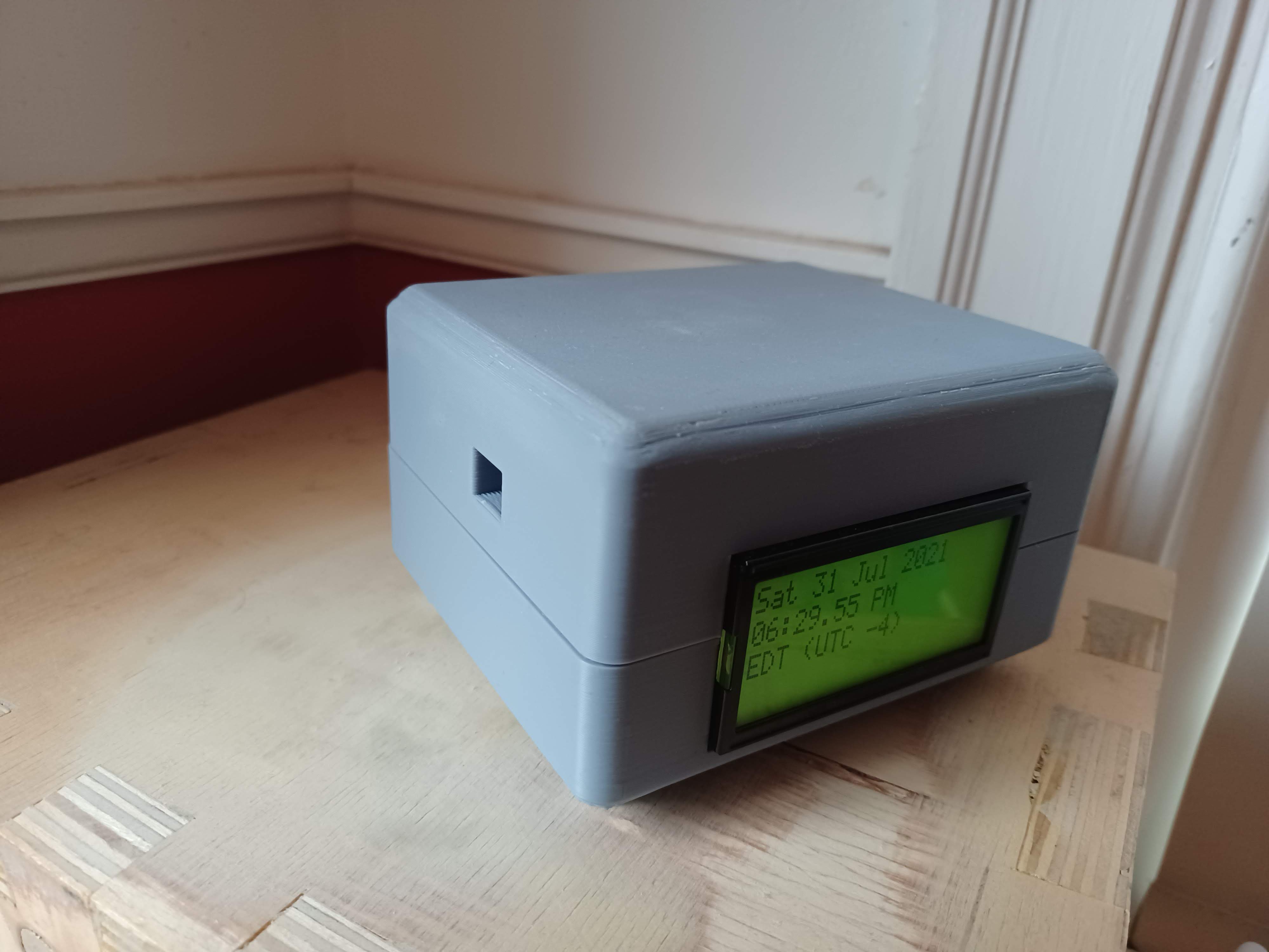
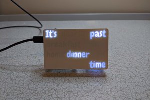
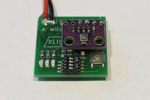
pictures of the finished device are spread throughout the project logs linked above.


 alnwlsn
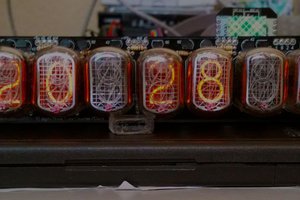
 ziggurat29
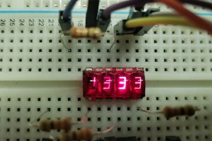
 Jeremy g.
wao its amazing: this watch display different others watch:https://vatcalculatorlive.co.uk/