 zaphod
As mentioned in a previous post the current version (v3.1) of the clock's main PCB didn't work completely. Specifically it caused the FPGA to burn up shortly after being plugged in. This was a pretty mysterious problem, since the FPGA didn't blow immediately, but instead seemed to work for a few minutes (I was even able to configure it once) before starting to draw a lot of current and burning out.
The problem was further compounded by the fact that the particular part number I had specc'd is on back order everywhere, and as a result I was unable to order more parts and do more testing. Additionally the parts I was initially testing with were in unknown condition, since they were originally bought for/built into the first hardware version that I started over a year ago, and hadn't been stored very carefully in the interim. Finally, it's possible that the flux I used during assembly was dodgy (all though this may just be paranoia).
Therefore it's time for some new board revisions.
Before starting on the next version I had to validate as much of the existing design as I could. I was quickly able to get the ATmega up and get it displaying stuff on the display thanks to some old code I had from the first pass at the project. I was also able to confirm that the ATmega ought to be able to talk to my verilog, provided I could get it running on a non-exploded FPGA. This was mostly covered in this log.
The final thing to validate was the FTDI UART/USB bridge. In the original (v1.0) design I had trouble getting the FTDI chip to survive for very long, likely due to a lack of USB protection, and so I had never written code to test bidirectional serial comms.
Fortunately the USB protection on the v3.1 board seems to be sufficient, and I was able to hack together some test code to confirm that I can send bits to the ATmega, and it can send bits back to me. (no picture here since it would just be a screengrab of `minicom` or `cu`).
Thus, I felt ready to begin designing new PCBs. Ideally, the device would use the LMCXO2-1200HC-4SG32C, which is exactly the FPGA in the tinyFPGA Ax2 devboard. Unfortunately the 1200HC is sold out everywhere, and so I needed an alternative. There are two obvious options
- embed a whole tinyFPGA Ax2 devboard
- find a similar part that is still in stock and redesign around it
Option 1 is obviously simpler and quicker, but doesn't give me the nerd-cred of having successfully embedded an FPGA on a PCB I've designed. Option 2 is certainly the hard road, but also presents a better learning opportunity (and maybe a better resume item :) )
At any rate it wasn't a clear decision, and so I decided to just do both options 1 and 2. Which takes a little longer, but doesn't cost much more since JLCPCB lets you batch PCB orders. Thus, option 1 became PCB v3.2, and option 2 became PCB v3.3.
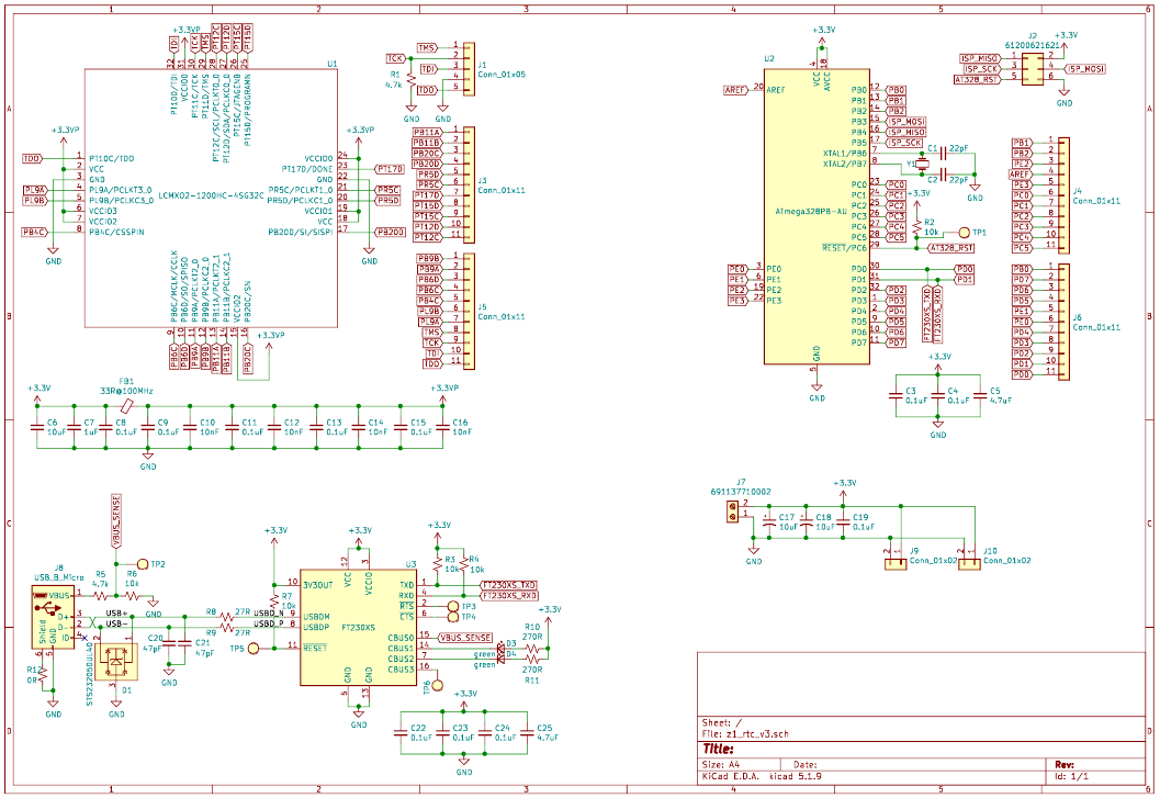
As a refresher this is the schematic for v3.1:
and this is the schematic for v3.2:
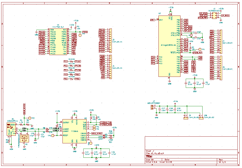
as you can see the v3.2 is a pretty simple replacement of the FPGA+support circuitry with the tinyFPGA-Ax2 module. The only other difference is the bank of 0R jumpers that are used to optionally connect some signals from the micro to the FPGA. Originally I had intended to just use the breakout pins to connect the micro and the FPGA, but the jumpers were easy to add, and will make the final design look a little neater.
For the v3.3 I needed to pick a chip I could actually order. After scraping through digikey and mouser, the cheapest (when considering shipping cost) similar chip I could order was the LCMXO2-2000HC-5TG100I, which is almost the same as the LCMXO2-1200HC-4SG32C, with a couple key differences:
- 2000 LUTs instead of 1200 (I was nowhere near topping out the 1200HC version, so this is pure overhead)
- TFQP-100 package instead of the QFN-32 (waaaaay more io than I'll ever need, but slightly easier to solder down I guess)
- a different speed grade, (series 5, instead of 4, rated for (I)ndustrial, instead of (C)onsumer use)
basically the new chip is complete overkill for what I need, costs like twice as much, and comes in a giant '90s style TFQP with a bazillion pins, but, I was able to buy it this year.
Thus, with my new parts in hand I went ahead and designed v3.3:
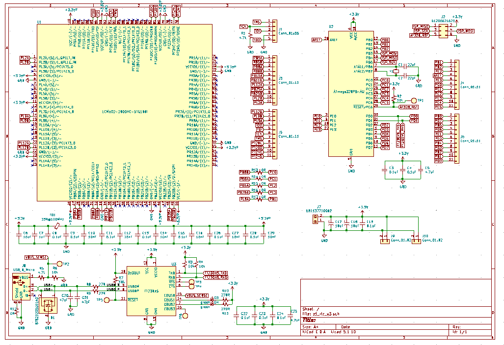
which is the same as v3.2 except with an FPGA and the associated support circuitry instead of the module. There will certainly be some sweat and tears required to get my verilog setup and running on the new FPGA, but hopefully it won't be too bad, and if it doesn't work I can always fallback on the v3.2 design.
After some quick layout I went ahead and ordered the boards from JLCPCB, and they should be here in a couple weeks.
If you're interested in finding all of the flaws in boards that I've already paid money for the designs are up on github here: https://github.com/ZakSN/z_1_rtc_pcb, there's a branch for each of v3.1, v3.2, v3.3 (see the readme).
As I mentioned in the last project log, the current FPGA design doesn't really work properly, there's a lot of things that it could be, but I suspect that its also a lot more complicated than it needs to be, and so I plan to try and audit the logic design while I wait for boards to arrive. I may also post a log explaining how the logic currently works, since I'll need to refigure it out anyway.
Discussions
Become a Hackaday.io Member
Create an account to leave a comment. Already have an account? Log In.