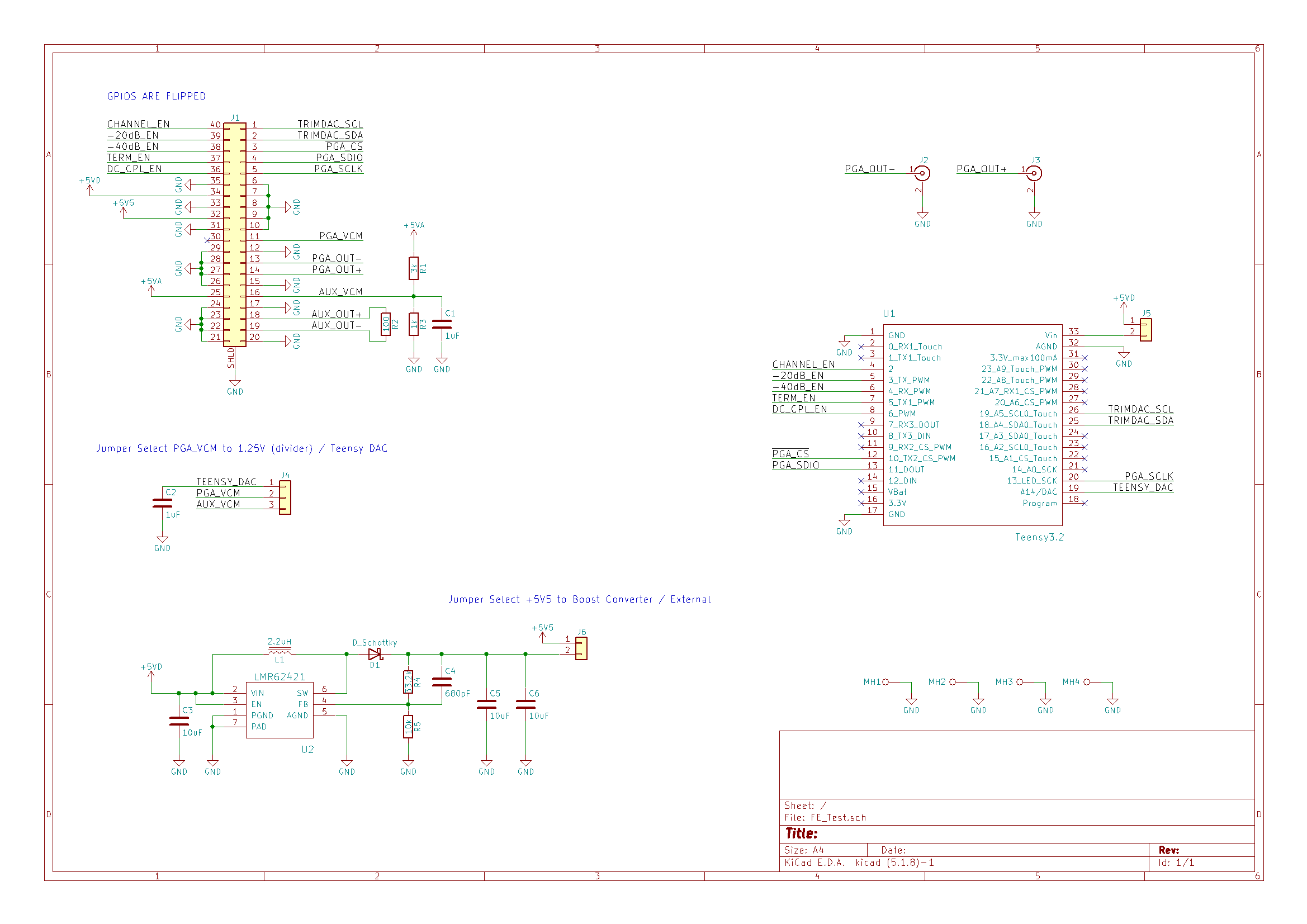
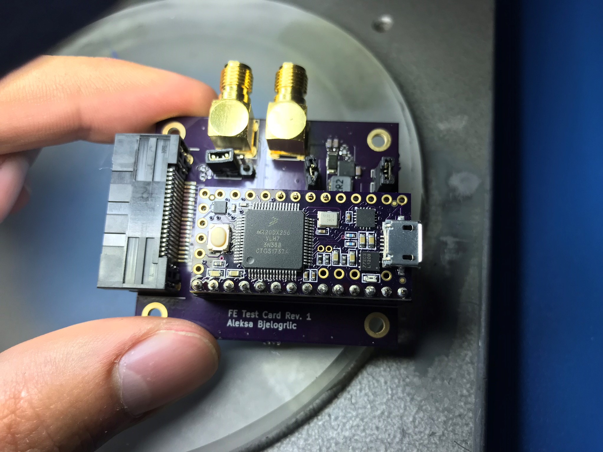
To evaluate the front end as a whole, I made a tester board for it. This board brought out the analog outputs from the PGA to SMA connectors and included a socket for a Teensy (microcontroller dev board, similar to an Arduino nano) to interface with the PGA, DAC and control signals.
 Aside from those main tasks, this board also stepped up the USB voltage to 5.5V, which was regulated back down to 5V for the PGA. This was done because USB VBUS voltage can drop as low as 4.75V, which is the minimum operating voltage for the PGA. When a linear regulator is added to "clean up" the voltage rail, the regulator's dropout voltage could cause the output to be below 4.75V, which the PGA isn't specified for. The common mode voltage for the PGA is also set on this board, for some reason I set this to 1.25V instead of the 0.9V needed for the ADC, but luckily enough I added an option to use the Teensy's DAC to set the voltage instead. In a classic blunder, I reversed the order of the GPIOs on the connector, but this could be flipped back in code.
Did I specify the Teensy just because I could get it in matching OSHpark purple? Yes, yes I did.

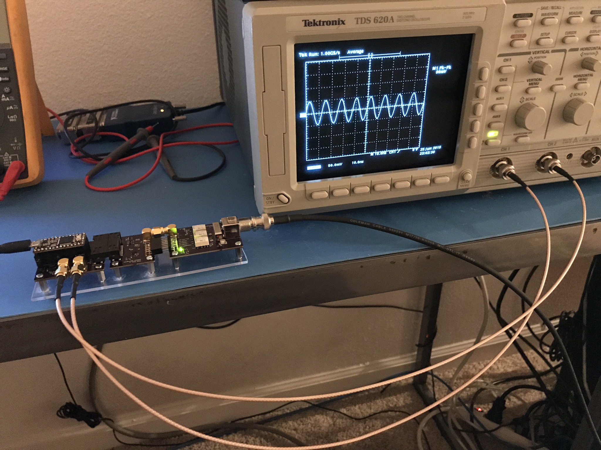
With all the boards connected, the tests could begin! As expected, the PGA (with its 900 MHz of bandwidth!) didn't impact the frequency response much. However, I noticed a flaw in my plans for the overall system when testing the values from my spreadsheet.
 Although the PGA was supposed to drive the ADC directly with about 1.8V full scale, it wasn't able to drive more than 0.9V at higher gains!
 This was, of course, in the datasheet! Tempted to repeat the mistake I made with Rev. 2 of the FFE board, I frantically scrambled to think of a solution. I looked for an ADC driver with enough gain to allow the PGA to output the 0.7V it was actually designed for, and give the ADC the 1.8V it needed. But having learned my lesson at that point, I took some time to really read over the ADC's datasheet. I found out it had built in digital gain that could be used for this task! The ADC actually samples at a higher than 8-bit resolution internally, so at low gains (in this case, ~2.5x) this feature had very little cost to overall performance, as the resolution with the gain applied was still greater than 8 bits. This enabled an entirely new architecture for the FFE! Until then, I elected to continue designing the rest of the system before going back to make the new front end. Next up, the ADC board!
Thanks for giving this post a read, and feel free to write a comment if anything was unclear or explained poorly, so I can edit and improve the post to make things clearer!
 Aleksa
Discussions
Become a Hackaday.io Member
Create an account to leave a comment. Already have an account? Log In.