 Aleksa
To stream the sample data as it comes it, it first needs to be converted into a format that the USB interface IC understands. USB interfaces generally come with specific applications in mind (e.g. USB to Ethernet, USB to SATA, USB to Camera Interface). If your application doesn't fit one of those niches, you must use one of the more general parts which typically use a 32-bit wide parallel interface. This is great for transferring any kind of data, regardless of protocol or type. However, our ADC does not have a matching 32-bit wide output. This means we need a device in between the ADC and USB interface to perform this conversion. A microcontroller would only take in data every clock cycle, which would require a blazing fast 1 GHz clock speed! A better choice for this task is an FPGA. These normally have a peripheral built in called a SERDES, which can take in very fast serial data and turn it into slower parallel data, acting as essentially a high speed shift register. FPGAs also have block memory which can be used to buffer the data so that small changes in transfer speed (caused by varying latency on the host PC) won't cause missing data. The FPGA can also take in commands from the USB interface and convert them to SPI and I2C commands to control the rest of the system.
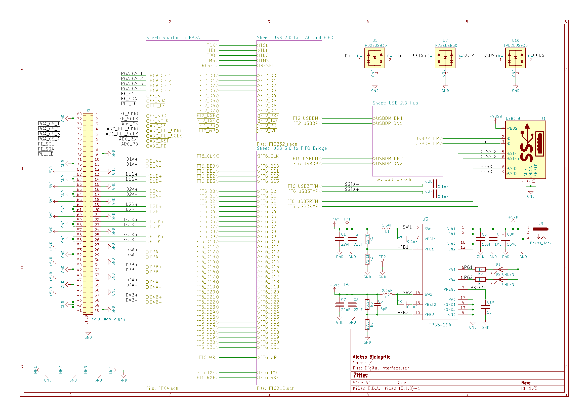 The main page of the schematic serves as a good block diagram for this board. The Spartan 6 LX4 FPGA from Xilinx was selected as it was the cheapest part that could handle the 1 Gbps LVDS inputs from the ADC. It also came in an easy to solder TQFP package and had just enough logic to do the basic tasks required of it, making it a perfect fit! I was going to use the Cypress FX3 line of USB interfaces, but I ended up switching over to the FT601 since it was a good deal cheaper and came in a QFN instead of a BGA package. This made it possible to inspect and fix soldering issues. I also read this excellent little whitepaper from Numato Labs which inspired me to use a separate USB 2 interface for side-band communication (like issuing serial commands to the rest of the board) and programming the FPGA. This whitepaper also had a neat trick up its sleeve: directly connecting the USB 3 RX/TX lines, while using a hub on the USB 2 connection! This saved me from using a USB 3 hub, lowering the cost and complexity of this board.
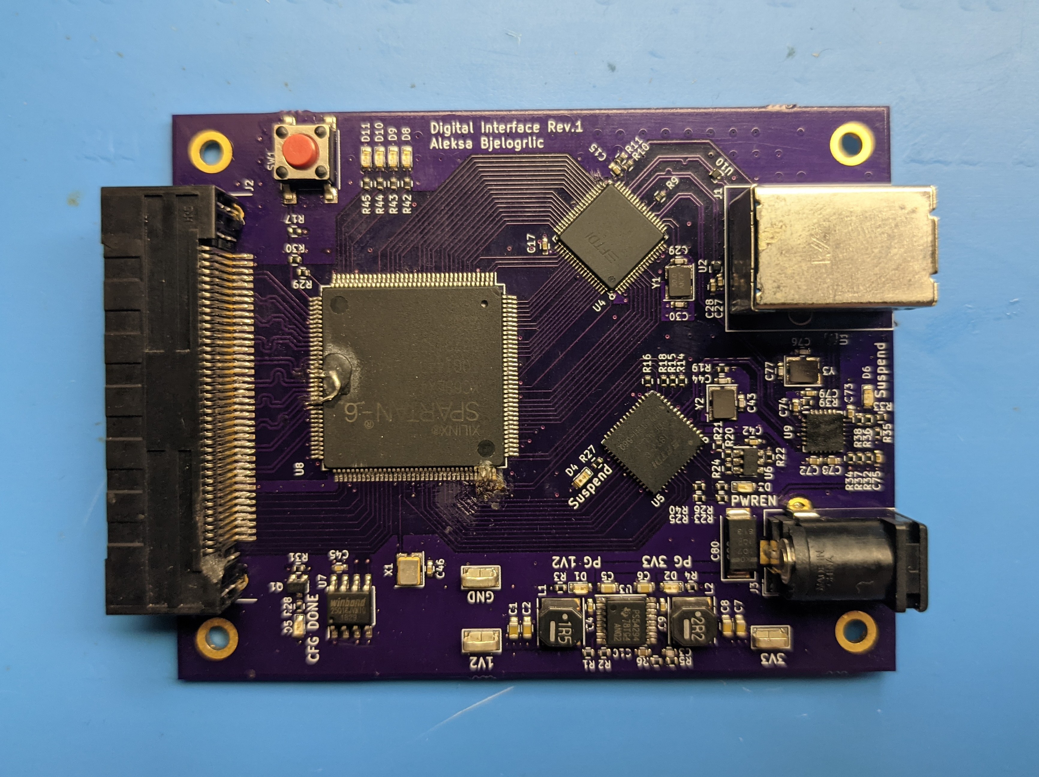
The numbers Mason! What do they mean? This was the first board that I added reference designators to, which are numbers that visually link parts on the board with their corresponding part on the schematic. This makes assembling and testing the board easier, as do the labels on the testpoints and LEDs. This was the first board I built for this project that I had a extra set of eyes on, which helped me catch some mistakes and improve the design as a whole. Huge thanks to my awesome co-workers at the time who reviewed the board with me!
Unfortunately some issues always slip through, so don't put too much pressure on yourself to make Rev. 1 perfect! One such issue on this board was a classic pin swap - TMS & TDO on the JTAG interface to the FPGA were flipped. This made the FPGA impossible to program! It didn't even show up in OpenOCD, the software I was using to program it. I eventually fixed this by lifting both pins and soldering them to the opposite pads, a fix made possible by the TQFP package of the FPGA.
This didn't fix all of my programming woes, as for some reason the FPGA wouldn't load a bitstream from SPI flash. This meant I had to program it through JTAG every time it lost power, which made for an annoying development process. After searching OpenOCD documentation, reinstalling drivers, and pulling half my hair out, I finally looked back through my schematics and found the issue! I had accidentally given the same pin number to both a regular pin (which I was using to receive ADC data) and one of the boot mode select pins. KiCad had given the connection to the ADC priority over its direct connection to ground for setting the boot mode, leaving the pin floating during boot. I soldered on a pulldown to set the boot mode correctly, solving this issue.
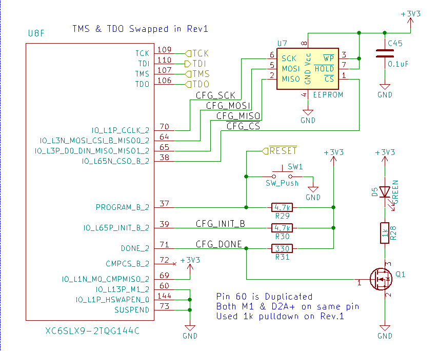
The configuration block of the FPGA - basically the only pins that you can't swap!
Now that I could program the FPGA, I needed to learn Verilog to get it to do something useful. In my next post, I'll cover every block inside the FPGA, the things I learned starting to code in Verilog, and the mistakes I made along the way!
Thanks for giving this post a read, and feel free to write a comment if anything was unclear or explained poorly, so I can edit and improve the post to make things clearer. I'd also like to thank Hackaday and the Hackaday prize judges for selecting this project as a finalist for the Hackaday Prize, I'm very excited to continue to write about this project as I work to improve it further and hopefully make an awesome open source oscilloscope for everyone on their electronics journey!
Discussions
Become a Hackaday.io Member
Create an account to leave a comment. Already have an account? Log In.
Congrats re your HaD Prize finalist selection! This is a pretty ambitious project and I appreciate reading through your process. I wonder how this will end up changing basic ideas of what oscilloscopes are/do – it seems like the sort of thing that could evolve in unexpected ways. Glad to see recent activity at GitHub & Discord where it looks like you & team are still pushing this along.
Are you sure? yes | no