 Aleksa
Learning to write code for an FPGA requires a change in mindset compared to programming for microcontrollers. You are no longer writing code to execute in order, but are describing hardware that the FPGA can reconfigure itself to be. This is why FPGA code is called HDL (Hardware Description Language), of which Verilog and VHDL are the two most common. I decided to use Verilog on this project and used these great tutorials from Alchitry to get started with it.
I decided to approach the FPGA design like I did with the rest of the project and broke it up into small parts that could be tested on their own before connecting them as a system. And just like the hardware for this project, I started off by making a block diagram to plan the design out.
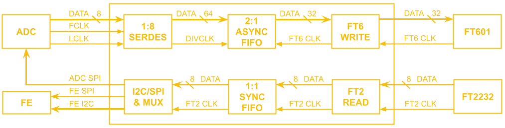
High bandwidth data flows only in one direction from the ADC to the FT601 USB 3 interface. This data comes in at clock rate too fast to process in normal FPGA fabric (fabric being the sea of logic elements that makes up the bulk of the FPGA) and must be "geared down" to a slower clock rate. This was done with a built in peripheral called a SERDES that takes in 8 bits of data at the higher clock rate (LCLK) and outputs them in parallel at 1/8th the clock rate (DIVCLK). These 8 bits may not all belong to the same byte, so the ADC provides a frame clock (FCLK) to synchronize the SERDES with the byte boundaries. Since the ADC has 8 lanes of serial data, each lane has a SERDES and all of the parallel outputs are combined into 64 bits of parallel data.
This data is then written to a FIFO, which does a few important things in this design. First, it changes the data width to the FT601's native 32 bits. Second, it provides that 32 bit data at the clock of the FT601, which is double the speed of, but asynchronous to, the divided ADC clock of the input data (this is a clock-domain crossing, which is a big deal in FPGA land!). And third, it buffers the data in the microseconds that the host PC takes between reads, which would otherwise result in lost sample data. Luckily enough, I could automatically generate a suitable FIFO in Xilinx's ISE tools. I only had about a few weeks of Verilog under my belt at that point, and I did not want to risk messing up such an important part of the design by writing it myself.
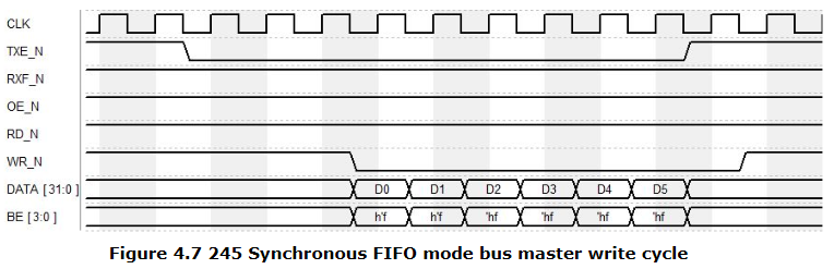
I wrote the FT6 Write block to work with the 245 Synchronous FIFO mode on the FT601 to write data to it. This was the simplest interface the FT601 offered, with only clock, data, and three control signals. When the PC requests data from the chip, TXE_N goes low (The host PC must poll the chip constantly to get a stream of data). The FT6 Write logic must then wait two cycles before taking WR_N low and sending the parallel data. The byte enable signal BE is always high since all the bytes need to be sent for maximum throughput.
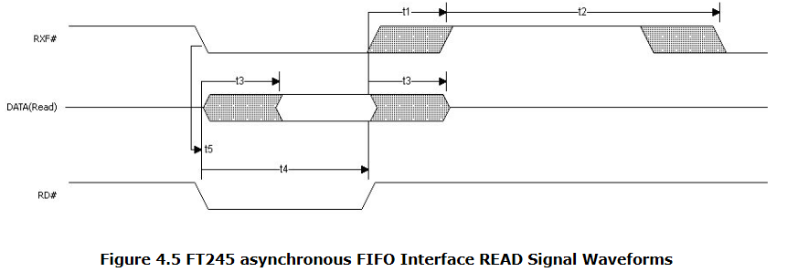
Moving on to the low-speed path, the module I started with was FT2 Read. The FT2232 offered a very similar interface to the FT601 with the option to forego a clock and operate asynchronously! I chose to use this asynchronous mode assuming it would be even simpler than the synchronous mode I used on the FT601. In a way I was right, all the FT2 Read block did was drop RD# low when RXF# was low, read a byte of data on the parallel pins, and pulled RD# high again. Then I encountered all sorts of timing issues since nothing was synchronized with the clock I was using (32 MHz, fed to the FPGA from an oscillator on the board). I didn't break out the pins needed to switch to the synchronous mode on the digital interface board, so I had to bandage together a fix on the FPGA. To do this, I ran the control signals through a synchronizer and clocked in the data based off of the now clock-synchronized signals. This worked, but still wasn't the most correct approach. I would recommend sticking to synchronous interfaces, and more importantly, routing out all the pins you can on the board so you don't lock yourself into a bad design decision.
The second FIFO in this design was a simple one. The input and output data widths were the same, and the read and write clocks were the same (making this a synchronous FIFO). I tried my hand at writing this one myself, which I did manage to do while searching madly through my old digital logic course notes! This FIFO allowed commands to be stored and then fed to the I2C/SPI transmit blocks in chunks of up to 256 bytes at a time, instead of the byte-by-byte flow of the interface from the FT2232.
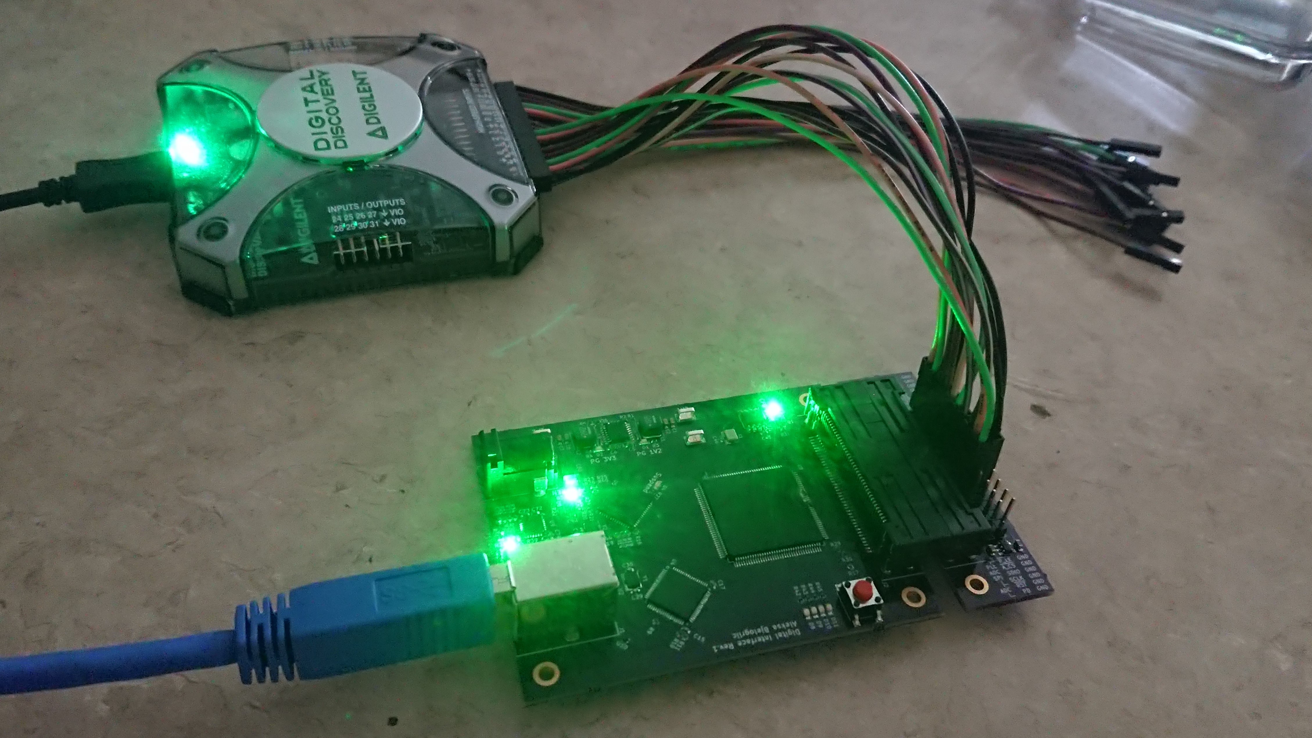
Before starting to work on the SPI and I2C blocks, I made a breakout board for the digital interface and attached it to a logic analyzer so I could verify that I was sending data correctly. I used state machines to handle the logic behind these protocols as well as counters to divide the main 32 MHz clock into 8MHz for SPI and 400KHz for I2C. The first byte sent from the PC selects which protocol the rest of the data will be sent through. If SPI is selected, it configures a multiplexer for the SPI transmit block to send commands to either the front end or the ADC.
With all the FPGA code written, It was time for the moment of truth! In the next post I will explain how I tested the system as a whole, touch on the software needed to get the first bits of data out, and the bugs I uncovered once I got the data flowing!
Thanks for giving this post a read, and feel free to write a comment if anything was unclear or explained poorly, so I can edit and improve the post to make things clearer!
Discussions
Become a Hackaday.io Member
Create an account to leave a comment. Already have an account? Log In.
Thanks for sharing Aleksa!!! I really like your modular design approach, and I think it’s brilliant that you took the time to test each module as you built it!! I’ve been thinking about building a scope for some time, and I am feeling inspired!!!!
Are you sure? yes | no
Glad to hear! I’m currently writing a post about all the testing on the system as a whole that I hope you’ll enjoy. You are also more than welcome to build off of my design for yourself (I’ll be releasing all the files once I document everything in the blog posts).
Are you sure? yes | no
I just wanted to say, I've designed PCBs for clients that used FPGAs/FIFO interfaces, but the way you laid this out made it a lot clearer for me what the use case is for such a thing. I don't get into the nitty gritty of programming very often, but it's useful knowledge for communicating with those outside of PCB-land.
Are you sure? yes | no
Thanks! They are great little chips for dumping whatever kind of data to a PC, downside is there's a lot to do on the software side of things. I'll try to give a good explanation of the software in a future post.
Are you sure? yes | no