 Aleksa
Now that I knew that the throughput to the PC could match the ADC’s rated sample rate of 1 GS/s, I had to make a circuit that clocked the ADC at that rate as well. This circuit needed to output at 1 GHz with very low jitter, as any jitter on the ADC sample clock will turn into noise during the conversion process.
The heart of the clock generation circuit is the phase locked loop (PLL). Without getting into too much detail, the PLL compares the phase of a low frequency reference (generally from a crystal oscillator) with a divided down copy of a high frequency that is generated by a voltage controlled oscillator (VCO), which it tunes until the two match. By changing the division settings any frequency can be synthesized, with the accuracy and jitter characteristics of the reference conferred onto the output.
Looking at the other scopes that use the same ADC, I found that many also used the ADF4360-7 in their clock generation circuit. I did some research on the part and it seemed to be the cheapest solution that would give me the 1 GHz output I needed. This chip had an integrated VCO, so the only other parts I needed were the reference oscillator and some passives. Saving me loads of digging into the datasheet, Analog Devices had a tool for calculating all the values of the passives as well as the register values to program for a given output frequency.
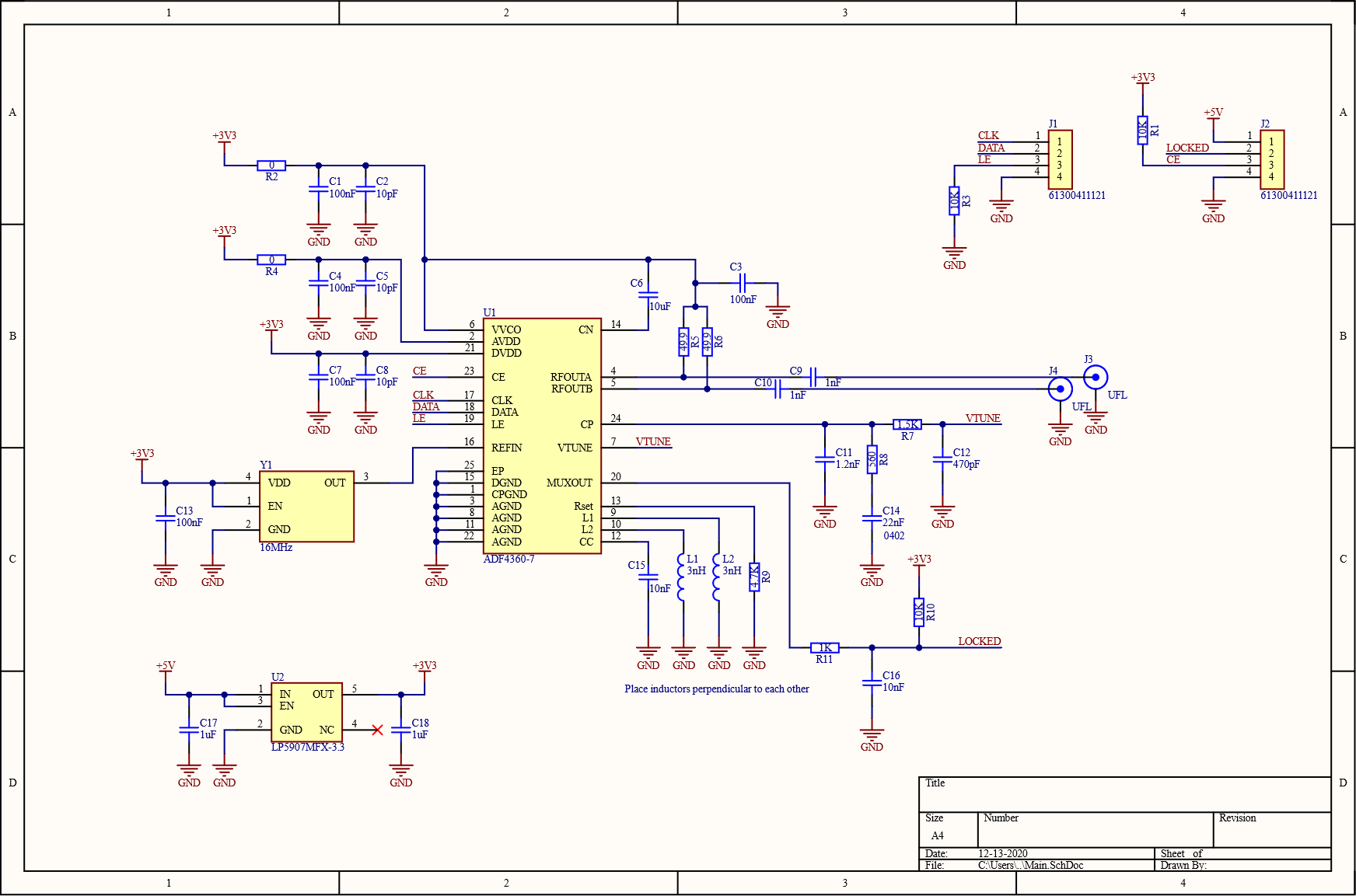
That sticky note yellow colour... The navy blue connections... That's not KiCad! It's true, it was at this point that I was offered an Altium license through my school. And with the size and scope of the next board already in mind, and the year of internships working with it, I decided to switch over. As for the design, I chose to use two 50Ω resistors (R5, R6) to bias the output as opposed to a more complicated matched network. The reference oscillator (Y1) was a 16 MHz crystal oscillator, which came temperature compensated for added frequency stability, and the LDO (U2) was a low noise part to avoid noise on the power rails affecting the performance of the circuit. Decoupling cap values were copied from the part's evaluation board and the rest of the passive values were taken from the design tool.
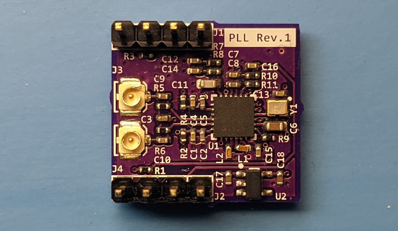
Pictured here, a 1 GHz postage stamp! I didn't have any decent way to test it on its own, so I hooked the SPI bus up to the rest of the oscilloscope prototype and updated the software to set all the registers on the chip at boot.
First I connected the RF output to a balun on a scrap ADC board to generate a single ended output that I could test on my spectrum analyzer. I then verified that it output at 1 GHz and used KE5FX's excellent GPIB toolkit to measure its phase noise performance against the simulation values from the tool as well as calculate total RMS jitter.
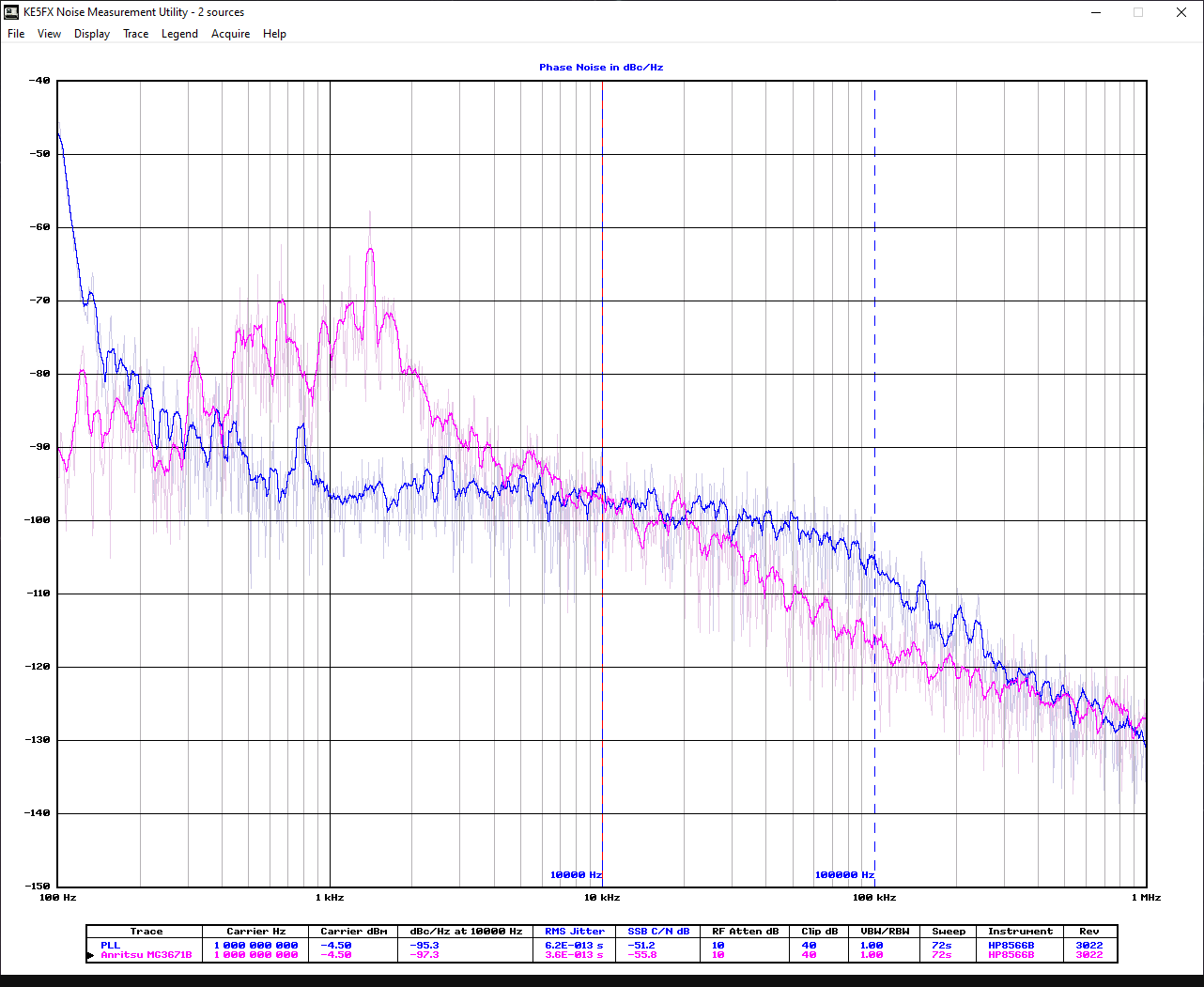
Here it is against my RF signal generator (in pink). The 100 Hz range was off, but the other ranges matched the simulations pretty well. The RMS jitter from 1.00kHz to 1.00MHz (didn't have a screenshot of this range, so the numbers are different here) was 760 fs vs. a simulated value of 580 fs. All of this looked promising, so I moved on to functional testing.
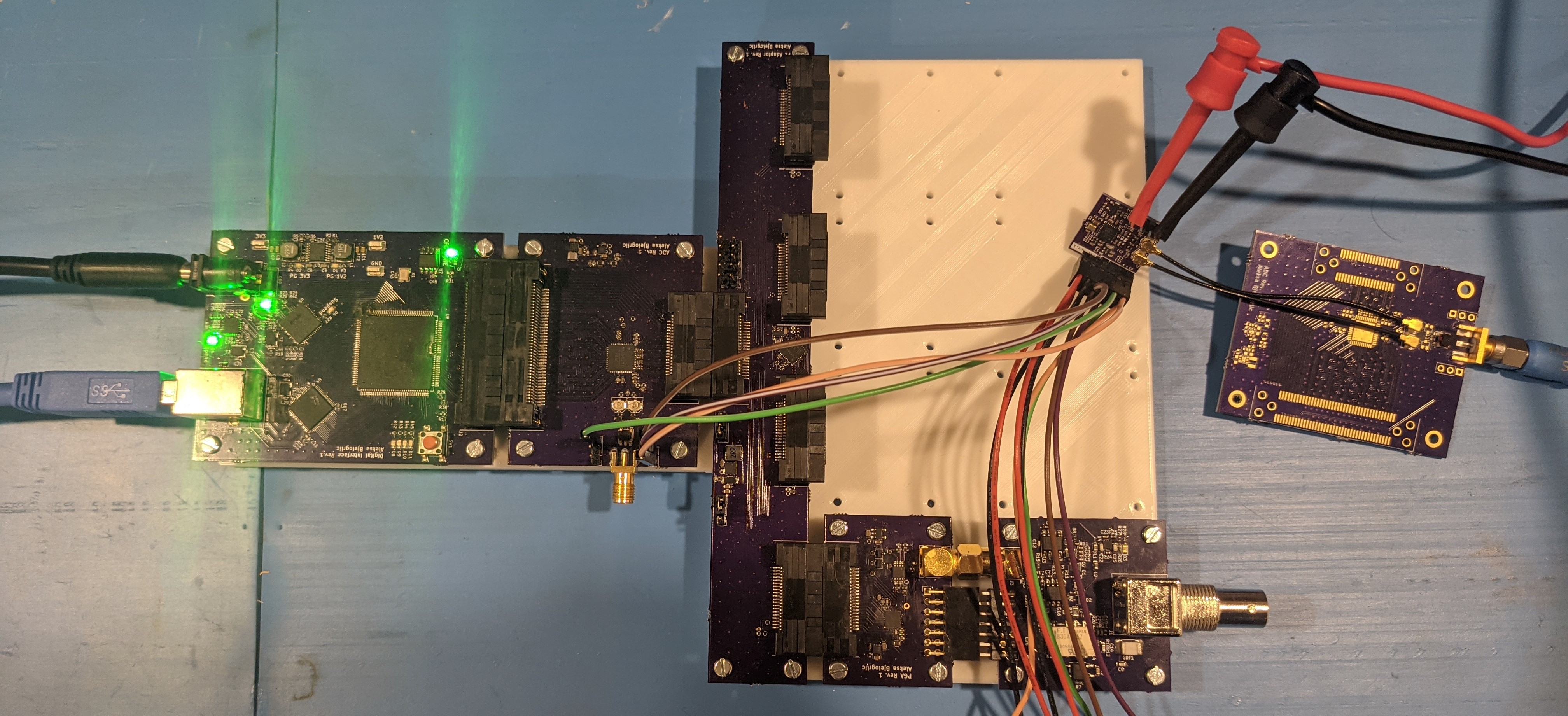
I hooked up the RF output into the ADC board through the two UFL connectors I included for differential inputs and updated the FPGA code to reflect the new clock rate. I then ran a quick capture to a CSV file, and the script hanged! That was odd, so I started debugging. Eventually, I found that the ADC wasn't outputting a clock at all! I looked through the clocking section of the ADC datasheet and this line jumped out at me:
"For differential sine wave clock input the amplitude must be at least ± 0.8 Vpp."
A quick trip to the dBm conversion table later, I found that I needed at least 2 dBm of output power. I had about -5 dBm! The matched output network I mentioned earlier would net me an output of -2 dBm according to the datasheet, which is still not up to spec.
My conclusion is that the circuit would probably work, given it's what the other manufacturers use, but it would have to be very marginal. The goal of this project is to make a better oscilloscope at the same price point by offloading so many costly aspects of a benchtop oscilloscope to the user's PC. This allows me to spend more on components to get the performance I want out of this design. With this in mind, I decided not to bother squeezing out every dBm just to reach the bare minimum the ADC would function on, and use a different clock generator that would make the most of the ADC.
Unfortunately, I was running out of time in my final term to get this project done. I had to go straight to the final design, a x4 PCIe card that incorporated all the other blocks I've written about, as well as a new (and untested) clock generator! Follow this project for the whopper of a project log that's coming up, as well as some posts about all the software work the rest of my group was doing as I was designing the hardware!
Thanks for giving this post a read, and feel free to write a comment if anything was unclear or explained poorly, so I can edit and improve the post to make things clearer!
Discussions
Become a Hackaday.io Member
Create an account to leave a comment. Already have an account? Log In.