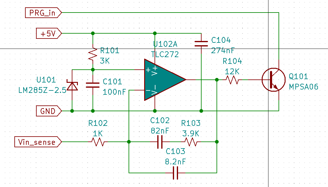
Close
0%
0%

Hardware MPP Tracking

A Method for Hardware Based Maximum Power Point Tracking

Similar projects worth following
Most MPP tracking is done by controllers in firmware. Various algorithms are used like the Perturb & Observe (P&O). Even when a DSP is used the MPP is disrupted because the controller must scan the PV's impedance in some way. This disrupts the DC converter's power delivery and reduces overall energy capture.

In reality the amount of energy loss is inmaterial, but what if MPP could be maintained continuously in hardware? This simple circuit does just that: U1 continuously adjusts the bias on Q1 to maintain Vref which represents the MPP voltage of the PV panel. The output of U1 at EAout is a voltage analog for maximum duty cycle. The circuit is driven by a small 'tracking' panel (in my test 50mm x 23mm) affixed to the main array.

Operation
U1 is an inverting controller that biases PNP transistor Q1 acting as a shunt across V3 (note the large value of C1 in the feedback loop: fast transient response is not necessary). V3 emulates the PV panel using a series resistance to deliver the expected current at the MPP voltage for the selected panel at MPP. V2 is set to the MPP voltage for the panel. In dark or low-light conditions the panel voltage will be less than Vref and EAout will be at Vcc (or whatever the + limit is for the selected op amp). Once the panel's output exceeds Vref, U1's output will decrease to bias Q1 and maintain Vref across V3 (e.g. Vload).

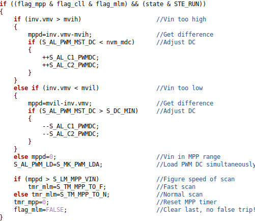
EAout can then be used to limit the maximum duty cycle of the DC converter to match its impedance to that of the PV array. The specifics of how this is done depend on the controller. With a Microchip PIC (or similar) the PRG, comparator, and COG peripherals can do this. The PRG is configured for a (-) slope ramp (same as slope comp) with its output driving one input of a comparator; the other input connected to the EAout signal. When the ramp equals EAout the comparator generates a falling event to the COG for duty cycle. The PRG's rate (V/uS) is adjusted to match the converter's switching frequency and MPP curve of the array. Another possibility would be augmenting the output of a VCO that drives a variable frequency converter.

The transfer function is:

    (Vref - Q1_Vbe) - (Q1_I / Q1_h_fe) * R3 = EAout

Q1_I represents the current thru Q1's emitter (or sourced from V3) and is an analog for the light energy imparted to the PV panel. Instability shouldn't be a problem since the combination of C1 and R3 keeps the gain below unity for anything greater than a few hundred hertz.

R3 should be set to ensure U1's output (EAout) can swing over the necessary voltage range needed to control duty cycle. At a minimum, it must be able to bias Q1 at MPP to maintain Vref with some margin. R3's starting value can be approximated by rearranging the transfer function:

    ((EAout - (Vref - Q1_Vbe)) / -(Q1_I / Q1_h_fe) = R3

Q1_I should be set slightly higher than MPP current. Also note the dependency on Q1's gain (h_fe): the data sheet's minimum value should be used.
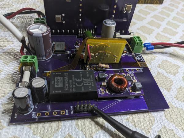
Validation
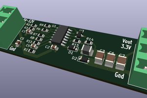
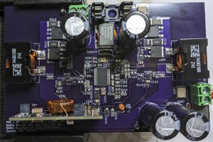
The circuit was prototyped using TI's OPA197 on an SOIC-8 breakout. Q1 is an old MPSA56, and the PV is Anysolar's SM141K07L monocrystaline PV (its values were used for the LTSpice simulation).

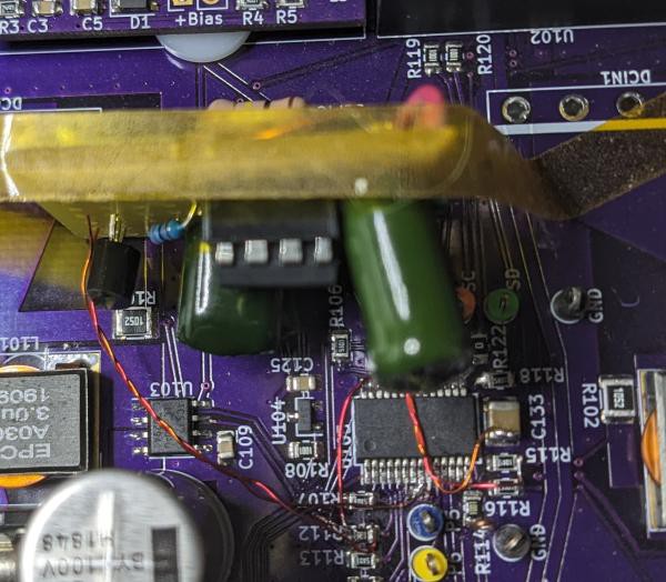
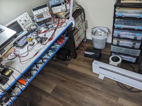
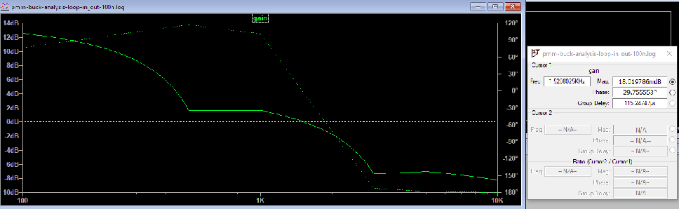
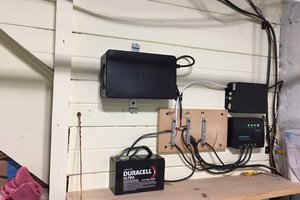
To more precisely measure EAout against the panel's output current the bench setup pictured below was used.

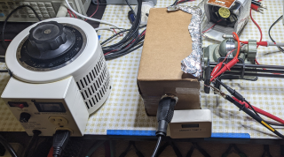
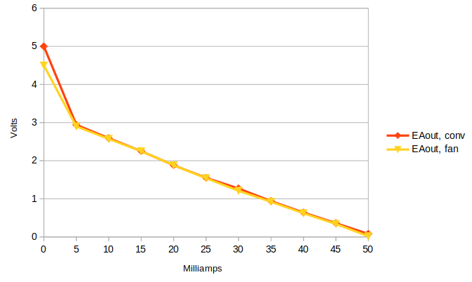
A VARIAC controls an incandescent bulb mounted in a box lined with aluminum foil that is focused on the panel. A cooling fan was used to provide more uniform measurements since PV panels derate at high temperatures. Below is a plot of EAout vs. PV current with & without cooling. They are nearly identical and, aside from zero output, are fairly linear.

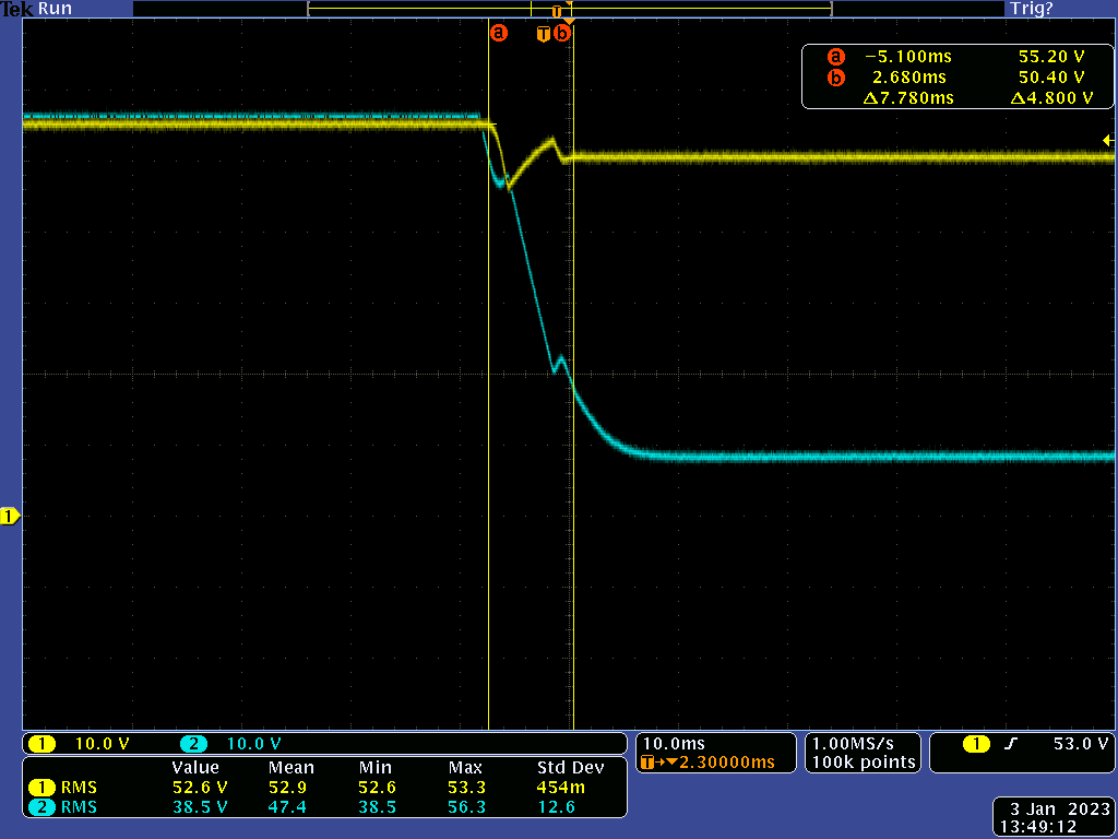
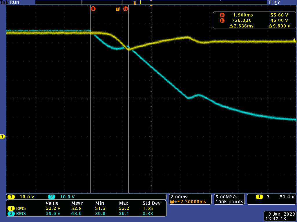
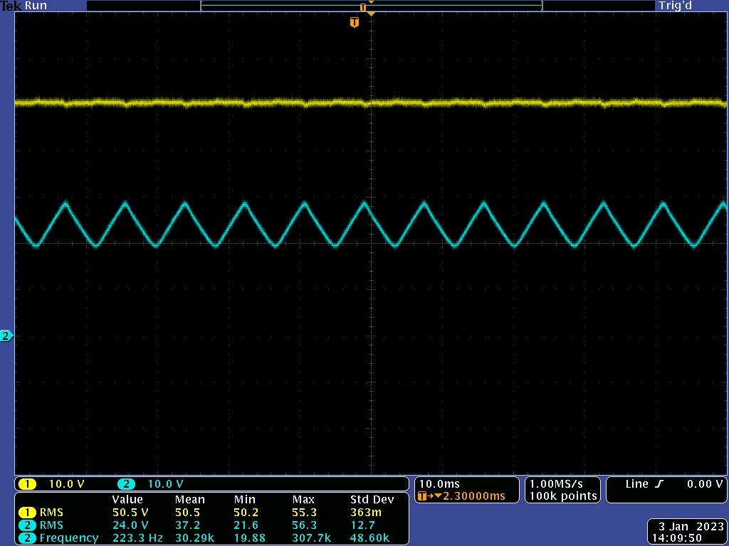
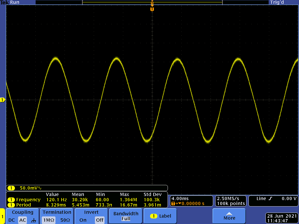
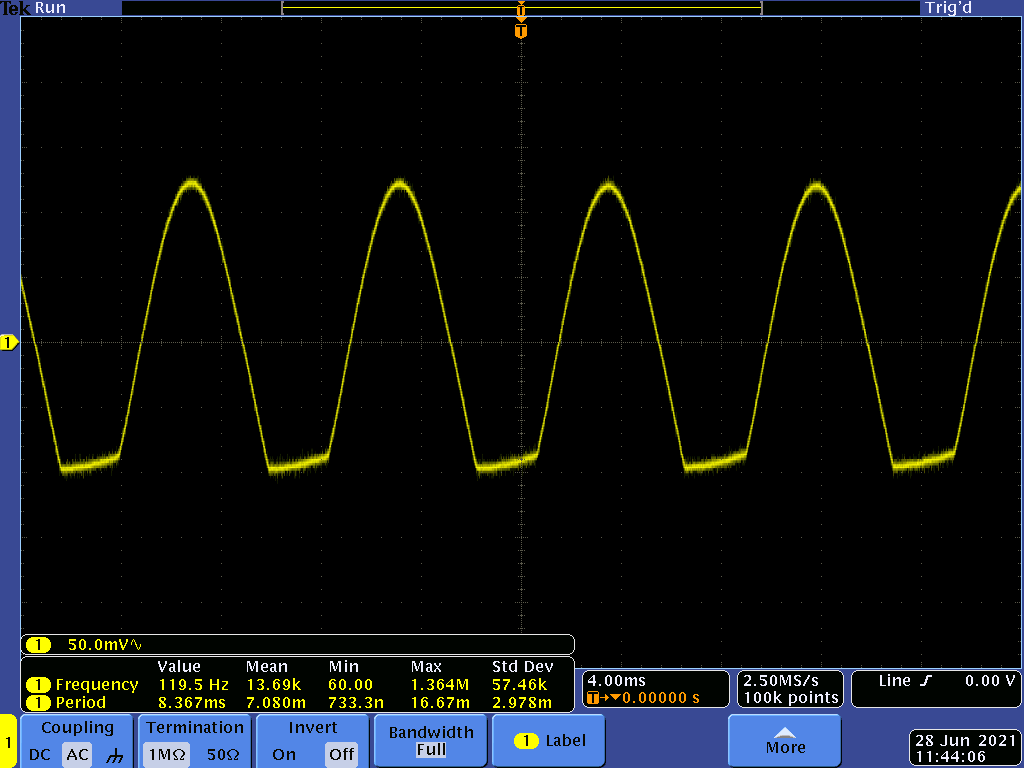
The two traces below show the OPA197's output. The first during a moderate load (~30mA) and the second approaching MPP. The negative output is clipping because R3's value is too high for the MPSA56' gain (minimum of 100 versus 200 for the 2SAR552P used in LTSpice). They are 120Hz sine waves because the bulb is powered from a 60Hz AC power source.

Implementation

This has not been tested with a working array and there are a number of considerations.

  • The tracking panel must be affixed to the array and requires additional wiring back to the controller / DC converter. DCR of the run length could affect operation. Noise pickup may require shielded cable and/or additional filtering.
  • This design will not work with installations subject to partial shading; the tracking PV must always be exposed to the same lighting conditions as the panels it represents.
  • The tracking PV's performance curve must match that of the array as closely as possible. This includes panel type [mono]poly-crystaline, temperature, and power coefficients.
  • This design functions as an open...
Read more »

mpp-buck-analysis-loop-in_out-100n.asc

Buck converter model with input & output control loops for evaluation of MPP tracking.

plain - 11.84 kB - 05/15/2022 at 23:23

Download

mpp-schematic.asc

LTSpice simulation.

plain - 1.87 kB - 07/08/2021 at 23:45

Download

  • Testing the Hardware MPPT Approach

    Brian Cornell01/05/2023 at 18:05 0 comments

    I finally got a chance to try the hardware MPP approach in a working converter. I used the prototype for my Solar Charger. I had to remove one of the SEPIC cores to make room and hack a few changes into the backplane.

    The MPP control loop is similar to the Closing the Loop (HW) log - a type 2 integrator with a zero at 500Hz and a pole at 5kHz. The phase boost is necessary because of a pole near resonance (~800Hz) between the input bulk capacitance and the SEPIC coupled inductor.

    A challenge with any multi-phase converter is how to servo the output control loops equally & simoultaneously, and is very dependent on controller architecture. It turned out to be easy with the PIC. The output voltage control loop is common to all phases and drives the ramp generators (PRGs) for each phase' inner current loop. Rather than trying to directly limit duty cycle as I had earlier proposed, the MPP loop simply subtracts voltage from the error amp's output to obtain a duty cycle that maintains the input voltage at the MPP value.

    A 1K resistor is placed between the error amp output and the PRG input pins and Q101's collector connects to the PRG side. R104 limits Q101's gain to the linear region. When the MPP loop engages, the PRG's input voltage is reduced which directly limits duty cycle. However, the output error amp knows no different - its gain & phase profile haven't changed. It sees the output voltage dropping and demands maximum duty cycle so, when the input voltage rises the converter's output power immediately increases.

    A few hacks to the charger's backplane and firmware were required to test this.

    Firmware
    • Disable output voltage sense.
    • Remap PRG inputs from controller pin 22 to pin 3.
    • Set input voltage measurement ratio to 20.
    Backplane
    • Remove R112 & C129.
    • Cut trace between R112 and via routing to bottom layer (output voltage sense must be kept intact to error amp).
    • Install 1K resistor at R112.
    • Add jumper from controller pin 22 to terminal 1 of R112 (30AWG magnet wire).
    • Change R103 to 549 ohms (~2.5V for Vin=50.5).
    • Add 100K resistor across pins 1 & 3 of J110 (to keep card over-temp from tripping).

    I built the MPP circuit on perf board using old parts I had lying around and used the power leads & polyimide tape to hold the board in place. Vin_sense connects to terminal 1 of R115, and PRG_in connects to terminal 2 of R112. Twisted pair (30AWG magnet wire) with a GND lead is used for both to maintain signal integrity.

    I don't have a Vector Network or Frequency Response Analyzer so I did the next best thing: beat on it with a variety of simulated input & output impedance variations to observe response & stability.

    This trace shows overall response with a static 4A load. CH1=Vin, 2=Vout. At cursor A the input impedance changes from 0.3 to 2 ohms. The MPP loop's overall response is just under 8mS and is reasonably damped.

    Same test but faster time base with cursor measuring loop's response before recovering to MPP value. Nothing to write home about but for MPP tracking I think this is decent.

    This trace shows MPP loop stability with a 120Hz impedance transient (1->4->1 ohm) applied to the converter's input. Vin holds steady at the MPP value with slight ripple.

    The acid test is how it performs with a real-world load. For this I connected a 48V DC -> 120V AC inverter to the converter. In turn, the inverter powered a 1.5kW space heater via an auto-transformer that allows me to control the AC load. The power supply for the converter was set to 57V with a 3.3A current limit. The inverter will place a time varying (sine) load on the converter and by applying enough AC load the input power supply's voltage will drop to engage the MPP loop.

    The only difference between this and a 'production' installation is the absence of a battery bank connected to the charger's output. This was intentionally omitted to place additional work on the MPP loop.

    CH3 is the converter's output current - note that it is sinusoidal but Vin (CH1) to the converter...

    Read more »

  • Closing the Loop (HW)

    Brian Cornell04/22/2022 at 21:21 0 comments

    One would think that the logical conclusion to this method is a hardware based approach. This log examines how it might work and what limitations apply.

    For simplicity, a buck converter with current mode control is used to model the MPP loop in LTspice. The current mode output control loop uses a linear ramp for slope compensation and a type-2 error amp to control output voltage. The comparator's output is gated to a flip-flop that drives the modulator and terminates the duty cycle.

    The MPP loop uses voltage mode control, also with a type-2 error amp. A linear ramp, calibrated to the maximum duty cycle of the modulator, provides timing for a comparator to terminate the duty cycle.

    The model includes voltage sources that can be modified to inject signals or transients to test stability and plot gain & phase margin. To measure gain & phase margin, comment out the '.tran' statement and set the 'parm t0...', '.tran', '.step', and '.measure' statements active. The frequencies to measure, and type of measurement, can be changed with the '.step parm Freq' statement. The sine voltage across nodes A & B must be set to 10mV and the variable {Freq} set in the 'Freq' field. Warning: the simulation can take hours, particularly at low frequencies. I believe that the linear ramps contribute to much of this.

    This gain & phase plot of the MPP loop shows a phase margin of just 29 degrees at a cut-off frequency of about 1.5kHz. Moving it down to 1.2kHz would likely get the phase margin up to a much safer 45 degrees. More could be done to increase phase margin and increase the cross-over frequency, such as resorting to a type-3 configuration. The input filter configuration for a given design will have significant influence on the bandwidth available for the MPP loop. For this simple buck with only bulk capacitance (no ESR is modeled) a single pole exists, so along with the error amp the maximum phase margin available is 90 degrees.

    For the tightest MPP tracking the loop should be slightly faster than the output loop, but with such a low cut-off frequency this isn't possible. Minimally, the MPP loop should be faster than load induced ripple, such as that caused by an inverter (120Hz).

    1.2kHz isn't fast for a SMPS control loop, but for MPP tracking it is likely fast enough to compensate for load induced ripple as well as environmental factors (e.g. shading, cloudy days, etc.). So, might it be better to stick with firmware? After all, it is easier to tailor the gain curve and add compensation for load, PV temperature, etc.

    The answer is that it depends on how well MPP must be tracked. Matching a 1.2kHz hardware loop requires sampling at least every few degrees. Sampling every four degrees is 9.25uS or 110KSPS. The sample set must be integrated and anti-aliased; either substantial computational overhead for the MCU or handled by a DSP. Hence, demanding applications that choose a firmware approach will require a fast MCU (100MIPS) with DSP.

    As previously shown, less capable processors can also use the firmware approach but must accept poor tracking in non-steady state conditions. Setting a MPP voltage range (as opposed to tracking a specific voltage) is a method for dealing with input voltage ripple induced by the converter design as well as load characteristics.

  • Closing the Loop (FW)

    Brian Cornell04/22/2022 at 19:38 0 comments

    I developed this idea while finishing work on the DC-converter section of my Solar Charger project. I needed an MPP algorithm for the firmware and didn't want to adapt the work that I had previously done with my Prototype MPP Charger - too slow. But, like that prototype, the Solar Charger's converter also uses an 8-bit PIC running at a measly 4MHz which will make any form of a P&O algorithm too slow.

    What if - instead of scanning for maximum power - the array's MPP voltage is maintained by the converter? For most PV panels, the MPP voltage does not vary significantly over temperature or load.

    No scanning required! The converter's impedance is limited to maintain the MPP panel/array voltage. This is incredibly easy to do, even on an 8-bit PIC, and requires just 28 lines of simple C code. Here's the snippet:

    The speed of this loop is controlled by a timer which is adjusted based on how far the converter's input voltage is from the MPP value. The converter's impedance is controlled by limiting the maximum duty cycle that the hardware control loop (to regulate the output) can demand. The two loops oppose one another but operate in tandem on the converter to form a closed loop. Note that in this implementation the MPP value is actually a range and not a singular value.

    This method has proven much more effective than my prior implementations using P&O algorithms, but it is still too slow (it is executing on the order of 100's of mS to a second or two). The result is that the input voltage (e.g. array Z) still crashes during load transients or partial shading conditions (but recovery is much faster).

    The variant pictured above executes in the foreground and there is room to go faster. This is ultimately governed by the speed of the infinite (I call it the RUN) loop, which would move its cut-off frequency to ~200-300Hz. You could go even faster by moving it to the background (ISR), limited only by processor speed and stable execution of other controller functions. With a faster processor, hardware equivalent performance may be achieved.

View all 3 project logs

Enjoy this project?

Share

Discussions

Similar Projects

Does this project spark your interest?

Become a member to follow this project and never miss any updates