 Tom
TomSuccess! The FPGA implementation can execute at least a few of the instructions at 100MHz on the Spartan Edge! Keeping in mind it's a simple test, running about 34 instructions: first, a bunch of LDI (Load Immediate) instructions load registers, then a combination of ALU instructions perform a sequence of ADD, SUB, etc. at various widths 8-bit, 16-bit, and 32-bit operations on registers, then NOP and a HALT, ending with the correct final results and flags. I can also step through the entire sequence of instructions one cycle at a time and watch the CPU stages, flags, and one register (r2) on the LEDs.

Here you see the final stage after running the test program. On the left 0b101 (stage 5 == HALT), then 0b010 (CPU Flags Carry/Negative/Zero so N flag set), and in red the low 8 bits of register r2 0b11111110 (-2 signed).
To see how I got here, we can look at the Logic Analyzer time view in Vivado. First, a few quick notes:
Currently, all implemented instructions take exactly 4 cycles, represented by the following Stages:
- pc_fetch - Request the next instruction from memory by promoting the value of the internal register nextAddress (which was set in the previous retire or reset stage) to curAddress, then assigning the memory bus address_out to that value for at least a cycle to load the instruction word
- decode - Load the new instruction word from the data bus data_in into the internal op register. All the appropriate connections to the ALU and other instructions are always wired, so they decode the result "immediately", available after only gate propagation delay in the same clock cycle.
- execute - Results of any operation (and appropriate flags and CPU states) are latched in internal registers. This is necessary especially in cases where one of the source registers is also the destination register location.
- retire - Write out latched results to the destination register, set processor flags, set nextAddress for the next pc_fetch.
There are also two others:
- reset - In this state while sys_rst is high
- halt - After executing a HALT instruction, stays in this state until sys_rst goes high. Useful for debugging/testing.
There are currently no wait/stall stages, as there are no memory or branch instructions so far, and I'm using Block RAM right now which always completes in 1 cycle, so we don't need to wait on a signal to read or write the memory value. Ultimately I will need to add these.

Now that you know what should be happening, let's look at it in the timeline. We will actually start on the last stage of the previous instruction indicated by the verticle line. Notice that nextAddress is incremented here to 0x00000004. If the previous instruction were a branch, it might have instead set the address to the branch target location at this point.

We now start the next instruction with the pc_fetch stage. Notice that the register curAddress is updated with the value of nextAddress, and address_out is wired to curAddress and the address 0x00000004 is sent out to BRAM.

One cycle later we are in the decode stage. Here we see that data_in now has the instruction word available, which is latched into the op register. This register is cleverly defined as a union of structs, each describing one type of instruction. These structs are in turn continuously wired to their respective logic so that when the 32-bit value is loaded into the register at the start of the decode stage, the results are computed for all possible instructions simultaneously in parallel in hardware. Only after we examine the opcode in the later cycles do we choose from the various results and write out only the information we need.
In this case, we have loaded an LDI instruction designated by op_ldi in the opCode field, so we can examine the LDI struct to see the contents of the instruction word. One bit labeled hiloFlag here determines if the 16-bit Immediate value immVal goes into the high or low 16-bits of the destination register (it is unset, or lowHalf in this case, immVal is 0xffff and the destination register is r2).
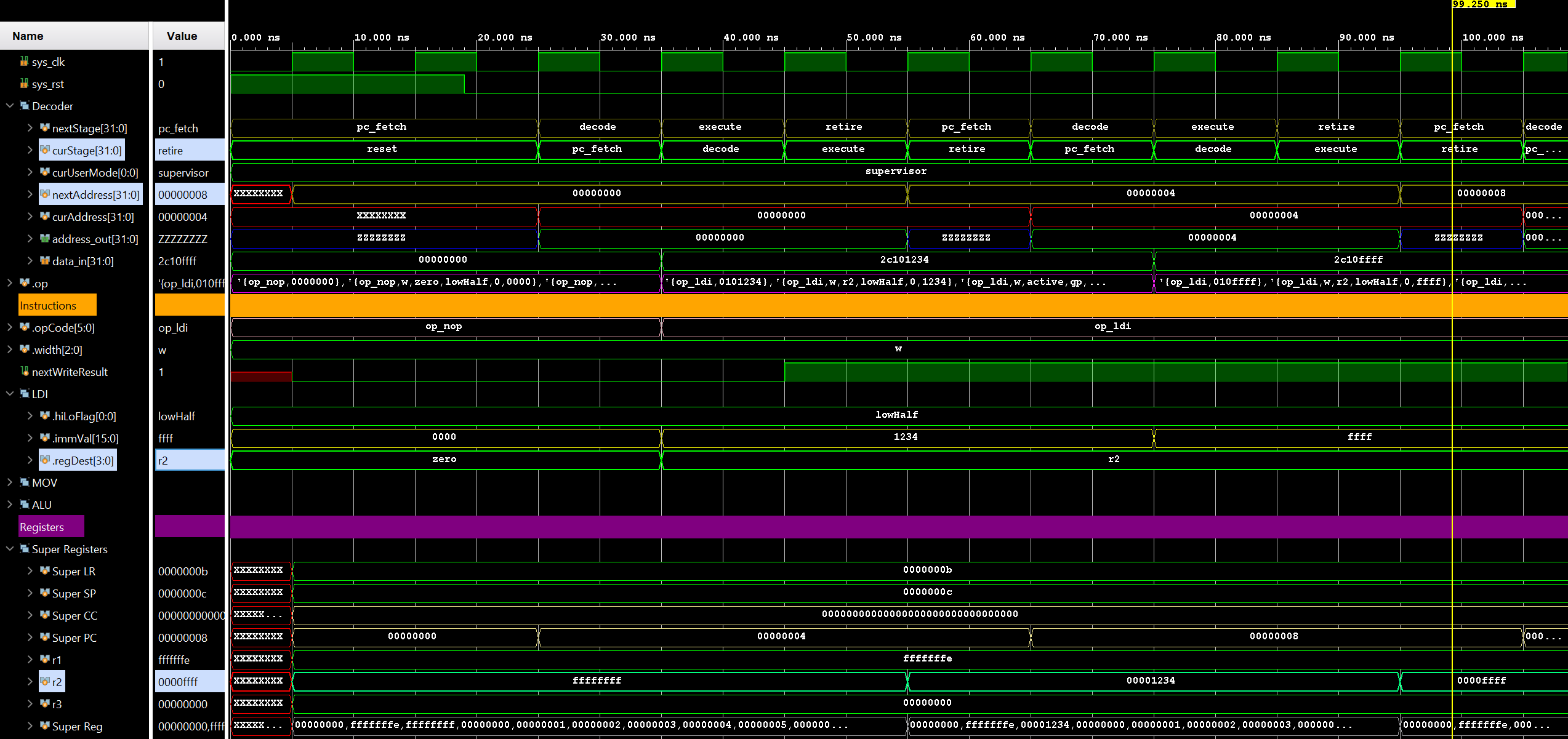
Nothing interesting happens in the execute stage for LDI, so we move on to the retire stage again. Here the CPU will write out the LDI result value of 0x0000ffff to register r2, update nextAddress to the value of the PC register (0x00000008), and finally increment PC to the next instruction address (0x0000000b).
This continues for the next 15 instructions, which are an assortment of LDI instructions to test different combinations of width, value, and registers. Then there is a similar sequence of ALU ADD/SUB instructions. I will cover those in the next update.
I am also working on an ISA document, but I'm only getting started...since I'm basically designing the CPU as I go...I hope to post more details on the instruction set and register architecture soon.
Discussions
Become a Hackaday.io Member
Create an account to leave a comment. Already have an account? Log In.