 Tim
TimThis is where things get a bit more interesting. I was concerned that it was quite difficult to coerce Yosys into using my custom gate libraries, but in fact it was rather easy.
The "cmos" example proved to be an excellent blueprint to creating a custom library. My logic family of choice is Resistor-Transistor-Logic (RTL), which is based only on resistors and transistors. Coincidentally, this is the same logic family that is used in the famous CDC6600 supercomputer. The basic logic element of RT-Logic is a NOR gate. Hence our design has to be implemented using inverters and NOR gates only. In addition, a storage element, a D-Flipflop, is needed.
Description of the logic cell has to be provided in the Liberty format. This format is quite comprehensive and usually also contains information about timing, area and wire loading. Luckily this information can simply be omitted which allows the library to be rather short and simple. The listing below shows the description of a NOR2 cell and a D-FF. The area line holds the number of transistors that are being used in this particular cell, hence the optimizer will try to reduce the number of transistors in the circuit. (In a real IC you don't care about the number of transistors, but mostly silicon area. For a discrete circuit on a PCB the number of transistors is more relevant)
You will notice that the DFF requires a whopping 15 transistors. This is indeed the minimum number of transistors for a "clean" DFF, as you will see later. There are some options to reduce this down to 7-8.
library(SingleLogicCells) {
  cell(NOR2) {
    area: 2;
    pin(A) { direction: input; }
    pin(B) { direction: input; }
    pin(Y) { direction: output;
             function: "(A+B)'"; }
  }

  cell(DFF) {
    area: 15;
    ff(IQ, IQN) { clocked_on: C;
                  next_state: D; }
    pin(C) { direction: input;
                 clock: true; }
    pin(D) { direction: input; }
    pin(Q) { direction: output;
              function: "IQ"; }
  }
}
The listing below show the yosys script to elaborate the design, perform technology mapping and optimization. Some intermediate output is generated as PDF file. The final output is stored in spice format, which turned out to be the easiest one to import to my placement tool.
# VHDL to Discrete logic


# elaborate VHDL code from GHDL
ghdl
hierarchy -check

# Rename top entity to 'main'. This is important, otherwise other parts of the flow may break.
rename -top main

# Draw netlist of elaborated design
show -format pdf -prefix 200_diagramm_hdl_elaborated

# Insert tristate buffers (ATTENTION: Currently not a supported cell type during P&R)
tribuf

# Technology mapping
techmap

proc; opt; fsm; opt;
dfflibmap -liberty ../20_SYNTH/discrete_logic_liberty.lib
abc -liberty ../20_SYNTH/discrete_logic_liberty.lib
opt_clean

# Print Statistics
stat -liberty ../20_SYNTH/discrete_logic_liberty.lib

# Draw netlist of optimized and mapped design
show -format pdf -prefix 208_diagramm_after_mapping


# Write out in spice format
write_spice 209_synthesized_output.sp
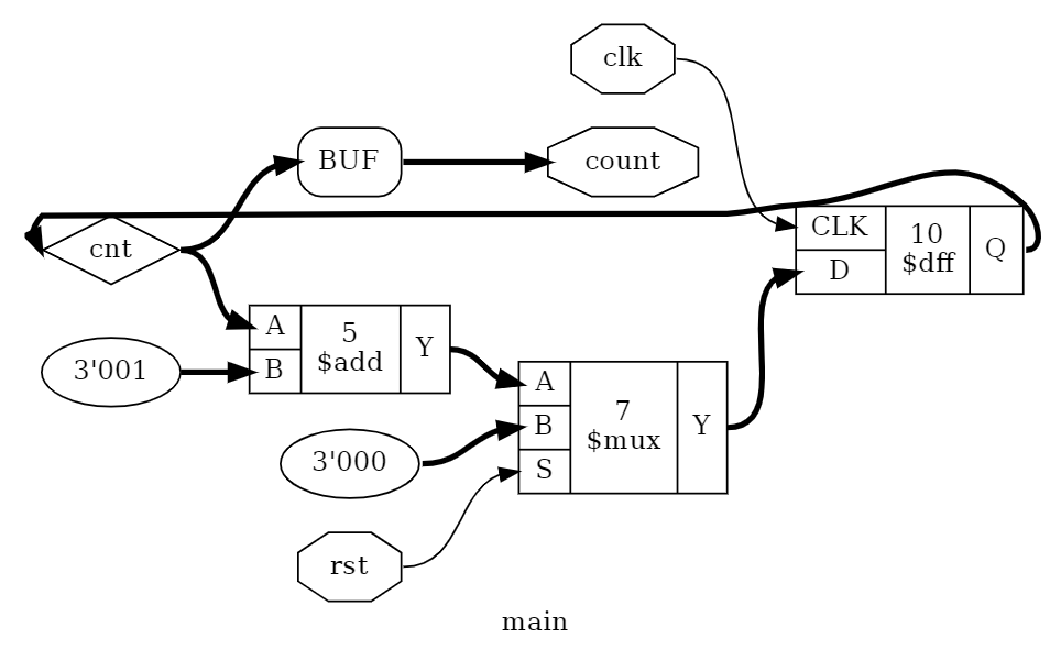
The counter design directly after elaboration.
 The counter design after technology mapping. All high level logic block have been broken down into simple gates.
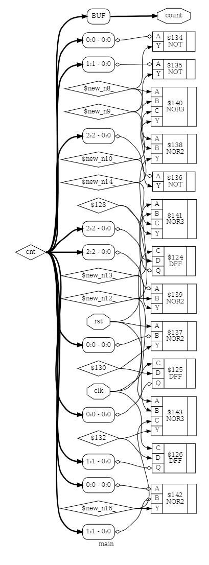
Finally, statistics of the design after the complete synthesis step. 13 logic cells have been generated, comprising a total number of 65 transistors.
13. Printing statistics.

=== main ===

   Number of wires:                 14
   Number of wire bits:             18
   Number of public wires:           4
   Number of public wire bits:       8
   Number of memories:               0
   Number of memory bits:            0
   Number of processes:              0
   Number of cells:                 13
     DFF                             3
     NOR2                            4
     NOR3                            3
     NOT                             3

   Chip area for module '\main': 65.000000
The spice output is relatively easy to read. Each of the "X..." lines corresponts to one logic cell including net names and cell type. As an extra quirk, voltage sources with "0V" are used to connect different nets.
* SPICE netlist generated by Yosys
.SUBCKT main clk rst count.0 count.1 count.2
X0 cnt.0 1 NOT
X1 cnt.1 2 NOT
X2 cnt.2 3 NOT
X3 rst cnt.0 4 NOR2
X4 1 2 5 NOR2
X5 cnt.2 5 6 NOR2
X6 1 2 3 7 NOR3
X7 rst 6 7 8 NOR3
X8 cnt.0 cnt.1 9 NOR2
X9 rst 5 9 10 NOR3
X10 clk 8 cnt.2 DFF
X11 clk 4 cnt.0 DFF
X12 clk 10 cnt.1 DFF
V0 cnt.0 count.0 DC 0
V1 cnt.1 count.1 DC 0
V2 cnt.2 count.2 DC 0
.ENDS main

************************
* end of SPICE netlist *
************************
Discussions
Become a Hackaday.io Member
Create an account to leave a comment. Already have an account? Log In.
Is there any "constant" extraction/minimisation ?
Are you sure? yes | no
Yosys and ABC do minimization very well.
What does not work that well is mapping to more complex logic gates. I thought about setting up a flow to map to single gate TTL logic, especially to the multifunction gates SZ57/SZ58. No success so far. But that's not an issue when mapping to resistor transistor logic.
Are you sure? yes | no