 Tim
TimBasic logic gate implementation
The synthesis step transforms the digital circuit into a spice netlist based on logic cells. To complete the circuit and allow analog simulation we have to actually implement the logic on devices level.
The most basic element of resistor-transistor-logic is an inverter. Logic levels are defined by the ratio between Rbase, Rload and the fanout, the number of gates connected to the output. To attain constant logic levels, it is therefore necessary to adjust the load resistor according to the fanout.
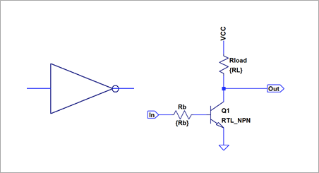
To work around this added complexity, I used a small trick, as shown below. The load resistor is moved to the input of the gate and the output is now "open collector".
This has two advantages:
- The logic levels are now independent of fanout, because the effective load resistance of the net will be reduced in proportion to the number of gates connected to it.
- Creating of NOR gates is possible by connecting the output of multiple inverters, without affecting the logic levels.
The only caveat is that an additional resistor has to be connected to the output of the circuit, if it is not connected to the input of another gate. For example if a TTL gate is connected.
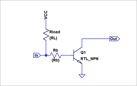
Below you can see the spice implementation of the basic inverter (NOT-Gates) and NOR2, NOR3 gates directly formed from it. This concept is extremely elegant, since our entire logic circuit can be implemented from a single basic element. Avoiding irregularity simplifies later steps like placement and routing.
.SUBCKT NOT A Y
Q1 Y N001 VEE 0 RTL_NPN
R1 VCC A {RL}
R2 N001 A {RB}
.ENDS NOT

.SUBCKT NOR2 A B Y
X1 A Y NOT
X2 B Y NOT
.ENDS NOR2

.SUBCKT NOR3 A B C Y
X1 A Y NOT
X2 B Y NOT
X3 C Y NOT
.ENDS NOR2
Latches and Flip Flops
HDL designs are typically based on registers, not latches. Hence a D-Flipflop is needed as a basic element. A D-Flipflop can be formed from two latches and an additional inverter for clock inversion.
To stay consistent with the logic family and reduced the number of transistors, I am using a polarity-hold latch as shown below.
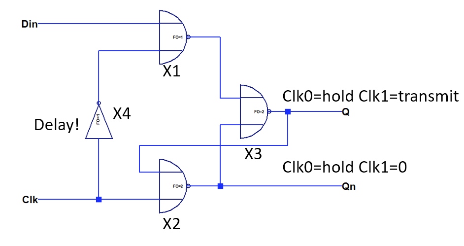
The function of the inverter X4 is to invert the clock. In principle, it could be shared beteween several DFF. However, the delay induced by the inverter is crucial to prevent an invalid state that casuses data corruption, therefore I opted to keep the inverter separate for each DFF. (See Earle Latch)
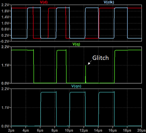
One nasty habit of the polarity hold latch is to introduce a glitch in the output for a rising clock edge when the output is zero. See spice simulation of a single PH-Latch below. Additional transistors can be spent to remove this behavior. Curiously this was also present in the CDC6600 (See thornton book).
The spice netlist for the polarity hold latch and a D-FF formed from two PH-Latches is shown below.
.SUBCKT DLATCH E D Q
X1 D nE N001 NOR2
X2 E Q nQ NOR2
X3 N001 nQ Q NOR2
X4 E nE NOT
.ENDS DLATCH

.SUBCKT DFF C D Q
X1 nC D t DLATCH
X2 C t Q DLATCH
X3 C nC NOT
.ENDS DFF
Testbench
Analog spice simulation can be perfomed using NgSpice. The testbench is shown below, it is directly based on the "cmos" example in Yosys. In addition to the logic cell library it also includes a transistor model.
* Spice testbench for discrete logic counterx
* Bases on Yosys "CMOS" example
* supply voltages
.global Vee Vcc
Vee Vee 0 DC 0
Vcc Vcc 0 DC 5
* load design and library
.include ../20_SYNTH/discrete_logic_spice_subckt.lib
.include ../20_SYNTH/RTL_NPN.lib
.include 209_synthesized_output.sp
* Define base and load resistor
.param RL=4.7k
.param RB=4.7k
* input signals
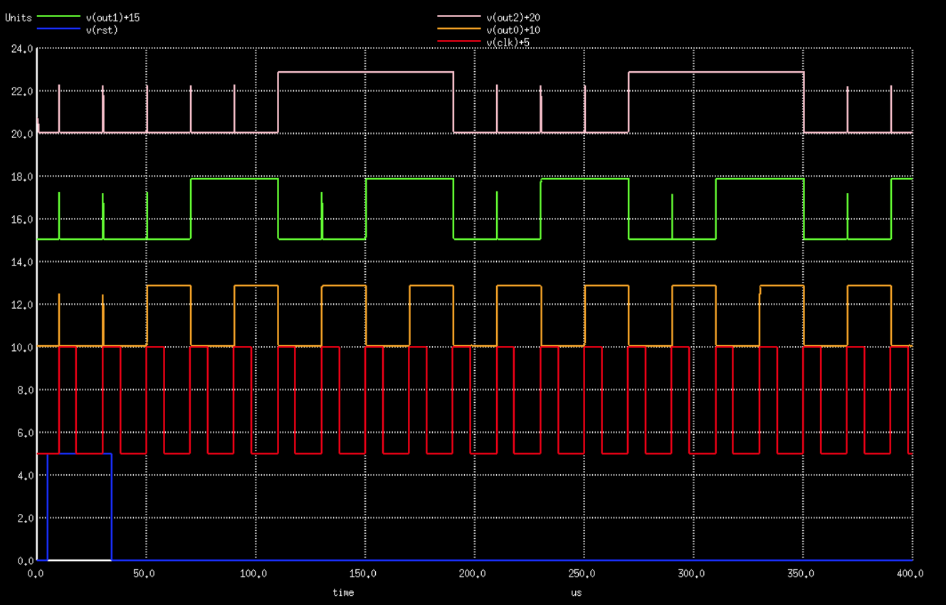
Vclk clk 0 PULSE(0 5 10u 20n 20n 8u 20u)
Vrst rst 0 PULSE(0 5 5u 20n 20n 29u 400u)
* Note: No pull up needed on outputs since they are internally connected. B
* Pull ups may have to be added for other designs
Xuut clk rst out0 out1 out2 main
.tran 20n 400u
.control
run
plot v(clk)+5 v(rst) v(out0)+10 v(out1)+15 v(out2)+20
.endc
.end
Simulation output is shown below. One can clearly see how the three bit counter counts up. In addition, the spikes caused by the polarity hold latch are visible.
Discussions
Become a Hackaday.io Member
Create an account to leave a comment. Already have an account? Log In.
would you consider adding a 50p cap in parallel with the base resistor ?
It's only a minimal price but not an insignificant speed boost, as long as you get the right cap value.
An optimisation of the resistor count & values, depending on the fanout, would be great too :-)
I believe some synthesisers can select the right gate according to the fanout and criticality of the signal. You might create several gates, each NOR can have 1 to 4 inputs and a fanout of 1 to 6 for example. That's 24 gates that can be generated by a double loop in a script...
Are you sure? yes | no
The way I chose the unit cell, no adjustment of resistor value is needed. Since the load resistor is at the input of gates, the effective value is automatically adjusted according to fan out. One could reduce the total numver of resistors by replacing parallel resistors with equivalent values, but this would mean that the BOM is balooning and would create a headache during footprint generation.
The idea with the cap is nice. I have not yet started to think about speed optimizations. But one could actually also add timing data to the liberty file and perform timing optimization. In that case also fast and slow gates can be picked by the optimizer during synthesis.
But alas, there are a couple of other things to tackle before. For example power grid optimization and automatic bypass insertion. Otherwise that will be the limiting part for anything fast :)
Are you sure? yes | no
The BOM will not explode : one resistor value per fanout. You could even roughen it up, with F01, FO2, FO3, FO45, FO67 ... that's 5 pull-up values.
Yes, power traces need to be way thicker :) Appropriate pour/fill is required.
And peppering the layout with 100nF capacitors would be a welcome addition :-)
Are you sure? yes | no
Right now I am only using a single resistor value. So having 5 instead would increase the BOM quite a bit. There are also issues with the spice models. One would indeed have to introduce many new subcell types. I was quite happy to find the short cut that allows me to work around all that complexity. So I guess I will keep that on the list for later optimization work :)
I still have not yet ordered a PCB build...
Are you sure? yes | no
You keep blowing my mind, dude !
Are you sure? yes | no
thanks :)
I have been thinking about setting up this flow for a year, probably. Took a lot of time until it "clicked" and i found the right short-cuts to make it actually work.
Are you sure? yes | no
it's well worth it !
Are you sure? yes | no