 Tim
TimOne issue of the logic style I am using currently is that a D-Flipflop takes up no less than 15 units cells, 15 transistors, 30 resistors. This has a huge impact on design size and it would be great to do something about it.
Months ago, I had a nice discussion with Yann on the TTLer HaD chat and we were competing in trying to reduce the number of transistors in a latch as much as possible. One amazing contraption that came out of this is the design below, that would certainly deserve a more detailed treatment than I can offer here.
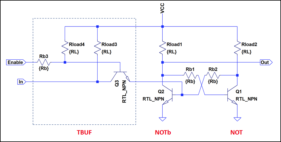 (Note: There is a slight mistake in the schematic above, Rload4, goes to the Enable input, not to the base of Q3). It basically consists of an R-S flipflop (the two transistors on the right side) and one transistor that is used as a pass gate. When the enable input is "high", the Input is able to pull up or down the base of Q2 since it has a lower impedance path. This type of latch design was common in the NMOS area (with a second pass gate to break the loop). Using a bipolar transistor as a pass gate is quite ugly due to asymmetric current gain, but it seems to work nevertheless.
 Maybe this is not the fastest option, but surely the smallest (so far). A DFF requires two latches and an inverter, driving to total transistor count to 7. Quite an improvement over the 15 of the earlier design based on polarity hold latches.
To implement this, it is necessary to introduce two new basic cells: TBUF and NOTb as indicated above. Both consist of one transistors and 2-3 resistors. There is one additional important point: To have a consistent impedance at the base of Q2, no additional load may be attached to the collector of Q1. This ensures that the pass gate works the same regardless of fanout. Therefore only the inverting output can be used. This is not an issue since we use two latches in series anyways.
Spice implementation below.
.SUBCKT NOT A Y
Q1 Y N001 VEE 0 RTL_NPN
R1 VCC A {RL}
R2 N001 A {RB}
.ENDS NOT

.SUBCKT TBUF E A Y
Q1 A N001 Y 0 RTL_NPN
R1 E N001 {RB}
R2 VCC A {RL}
R3 VCC E {RL}
.ENDS NOT

.SUBCKT NOTb A base Y
Q1 Y base VEE 0 RTL_NPN
R1 VCC A {RL}
R2 base A {RB}
.ENDS NOT

.SUBCKT DLATCH3Tn E D Qn
X1 E D N001 TBUF
X2 N002 N001 Qn NOTb
X3 Qn N002 NOT
.ENDS DLATCH
Discussions
Become a Hackaday.io Member
Create an account to leave a comment. Already have an account? Log In.
I'm eager to see it working for real !!!
Are you sure? yes | no
It's working, i got the pcbs today.
Are you sure? yes | no