 Tim
TimAutomatic synthesis of digital circuits has been the domain of very expensive electronic design automation tools in the past decades. Since a few years, there seems to be considerable momentum to develop and make available free toolchains for ASICs and FPGAs.
Notable projects
Yosys is probably the project that started the renewed momentum in free EDA tools. Is a versatile framework for logic synthesis and initially targeted a verilog to FPGA flow with a backend specific to lattice FPGAs. In the mean time this has been extended to SymbiFlow an open source toolchain supporting many FPGAs. ghdl-yosys-plugin is a plugin based on GHDL that brings VHDL support to Yosys. (So I can achieve my goal of being able to use VHDL).
Is a verilog to FPGA toolchain with a freely configurable backend allowing to explore different FPGA architectures, which is in contrast to Yosys which is somewhat hardcoded for specfic FPGA architectures. It is based on a different logic synthesis tool, Odin II.
I pondered for a while whether it was possible to adapt a FPGA toolchain to create PCB based designs. The idea would be to provide a matrix of fixed functional elements and let the toolchain do the routing. Unused elements could be removed later. In the end I did not pursue this route since the toolchains are heavily geared towards working with larger functional elements (e.g. LUTs), which cannot be easily implemented in discrete logic on a PCB.
Qflow is an open source synthesis flow targeting integrated circuits, that combines several preexisting tools to a full workflow. It is available from http://opencircuitdesign.com/. Yosys or Odin II is used for synthesis, Greywolf for placement and routing, qrouter for routing.
The OpenLane flow is another digital design flow that picked up a lot of momentum and sees a lot of activity. It uses Yosys as the synthesis frontend and a newley developed tools, OpenROAD app, for placement and routing. The flow supports the /skywater-pdk, an open process development kit for a 130 nm CMOS process.
Lists of open source EDA tools:
open-source-cad-tools
eda-collection
Adopting an ASIC flow?
The problem of synthesizing digital logic for a PCB is actually very simular to synthesizing logic for an integrated circuit.
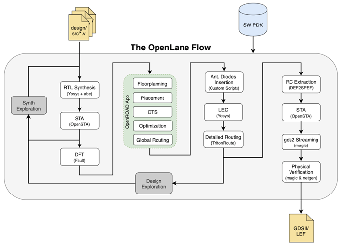
The image above shows the architecture of the OpenLane Flow (taken from here). The input to the flow is a our design file and a description of the technology, the PDK. At each step in the flow, the design is transformed in some way and saved in an internal representation until finally a layout file is generated. There are some feedback loops were tools parameters have to be finetuned to optimize the result.
Let's go through it step-by-step. Normal text is the OpenLane flow, italics are my thoughts.
- Synthesis
yosys- Performs RTL synthesisabc- Performs technology mappingOpenSTA- Performs static timing analysis on the resulting netlist to generate timing reports
This step takes the Verilog/VHDL source and turns it into a list of logic gates. The critical step here will be to define a set of logic gates that can be implemented in discrete logic and convince the tool to map to only these gates. Timing analysis is a step we will skip for now as the focus should be to get a functional circuit at first. Improvement of maximum clock speed could be a later optimization.
- Floorplan and PDN
init_fp- Defines the core area for the macro as well as the rows (used for placement) and the tracks (used for routing)ioplacer- Places the macro input and output portspdn- Generates the power distribution networktapcell- Inserts welltap and decap cells in the floorplan
The floorplan prepares the area where the synthesized logic goes and creates the power network. As a first step I will treat the power network as a normal net, which should be acceptable if performance is not a goal. A big question is wether the tools can be repurposed resued in any way.
- Placement
RePLace- Performs global placementResizer- Performs optional optimizations on the designOpenDP- Perfroms detailed placement to legalize the globally placed components
Places the predefined logic cells in a grid into the predesignated area on the IC. A critical step is to optimize the arrangement of the logic cells to minimize the length of interconnecting wired needed. We would have to do the same for the PCB and write the component footprints and placements. For our PCB flow, the output of this step should be an unrouted PCB.
- CTS
TritonCTS- Synthesizes the clock distribution network (the clock tree)
Optimized timing of the clock destribution network. For the PCB based flow we can treat the clock network as any other in a first step. This will only work if we can make sure that we have logic that cannot create unwanted conditions as a results of different timing. The easiest way to ensure this is to use D-flipflops.
- Routing
FastRoute- Performs global routing to generate a guide file for the detailed routerCU-GR- Another option for performing global routing.TritonRoute- Performs detailed routingSPEF-Extractor- Performs SPEF extraction
Routing of interconnects. Tools for ICs typically rely on many routing layers and detailed rules to optmize the routing. Since there are already many autorouters available for PCBs, the first step would be to use an existing tool.
- GDSII Generation
Magic- Streams out the final GDSII layout file from the routed defKlayout- Streams out the final GDSII layout file from the routed def as a back-up
This step is akin to generating the Gerber files for PCB manufacturing. There are many tools available for PCBs, so this should be solveable.
- Checks
Magic- Performs DRC Checks & Antenna ChecksKlayout- Performs DRC ChecksNetgen- Performs LVS ChecksCVC- Performs Circuit Validity Checks
Design rules checks are also available for PCBs, so we can rely on existing tool.
Discussions
Become a Hackaday.io Member
Create an account to leave a comment. Already have an account? Log In.