 Tim
TimThe fully assembled PCBs arrived a bit quicker than expected. Time for some testing.
Lesson 1: Using 5mm pitch instead of 0.2"" is quite annoying if you want to attach pin headers. I might adjust cells spacing or even insert the I/O pins at a pitch of 0.1"".
15T-DFF Resistor Transistor Logic Counter
The counter using 15 transistor D-Flip Flops is shown below. It uses 65 transistors and 130 resistors in total. I used a relative high load and bias resistance of 4.7k and the lowest cost transistors I could find, MMBT3904 clones from a chinese supplier. These transistors are only 0.0075 USD/pc for 200+, but have a rather long storage time, as I already realized in my Transistor Pixel project.
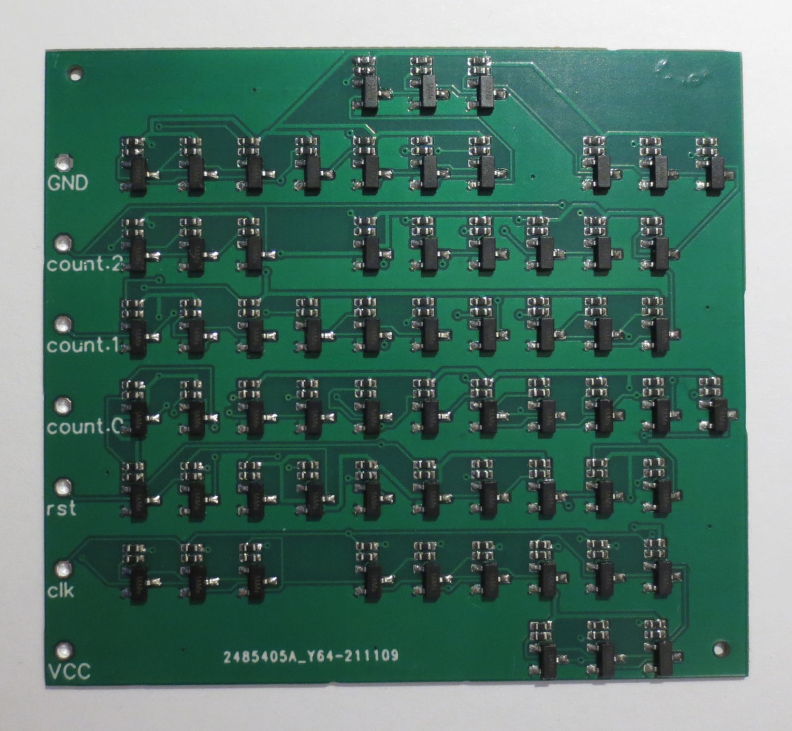
The static power consumption is 47 mA at 5V, still quite moderate for resistor transistor logic.
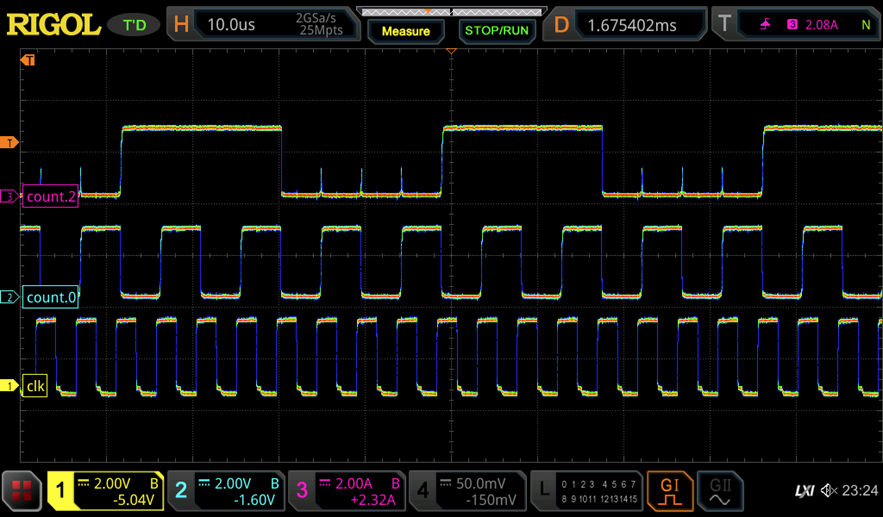
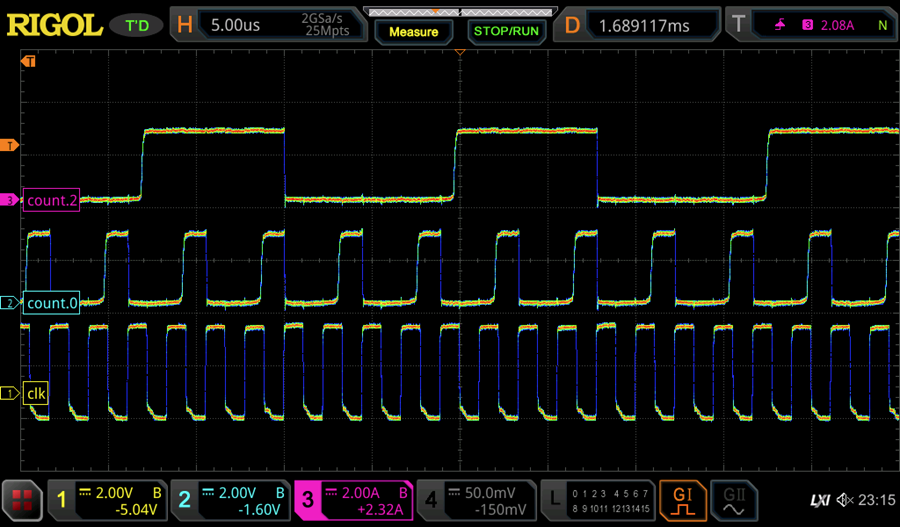
The counter is shown in operation above. Everything seems to work fine and according to simulation. Even the spikes from the polarity hold latch are clearly visible in the count.2 output. Generally, very little power nose is visible, despite now using any capacitors. The low slew rates of the gates probably help quite a bit with this.
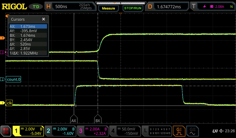
Clock to output delay is around 520 ns. The path from clock to output is 2, respective three inverter delays. Due to the storage time, a H->L on an inverter is transmitted much slower than a L->H. Luckily, the used latch structure equilized the delay regarding of data input; delay is the same for both latch inputs. Cray/Thornton certainly knew why they used this latch design in their CDC6600 By design, there is always one slow inverter in clock path, so we can assume that tpd is somewhere around 400-500 ns.
The maximum clock speed is 650 khz. It would be easily possible to speed this up quite significantly by using faster transistors (e.g. PMBT3904 or PMBT2369) and/or reducing load resistor. I opted to go for safety this time.
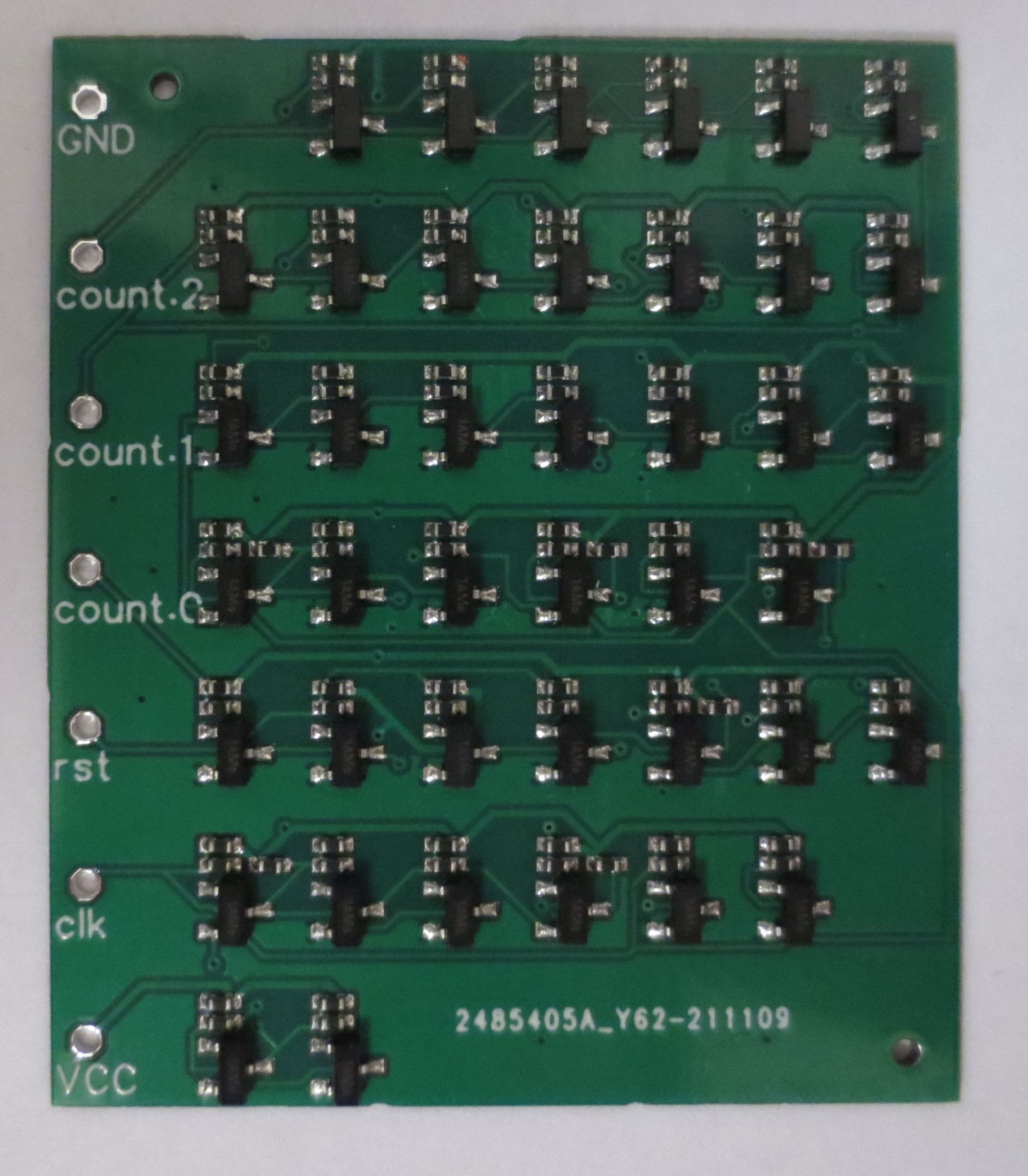
7T-DFF Resistor Transistor Logic Counter
The implementation with 7 transistor D-flip flops is shown below. It is much smaller, requiring only 41 transistors and 88 resistors. Due to this, the average current consumption is also a bit lower at 35 mA.
Operation of the counter is fine, as can be seen above. The three transistor pass-gate latches do not exhibit any spikes, which is much nicer. One can see a bit of crosstalk though (most likely through the pass transistor), which was also visible in the simulations.
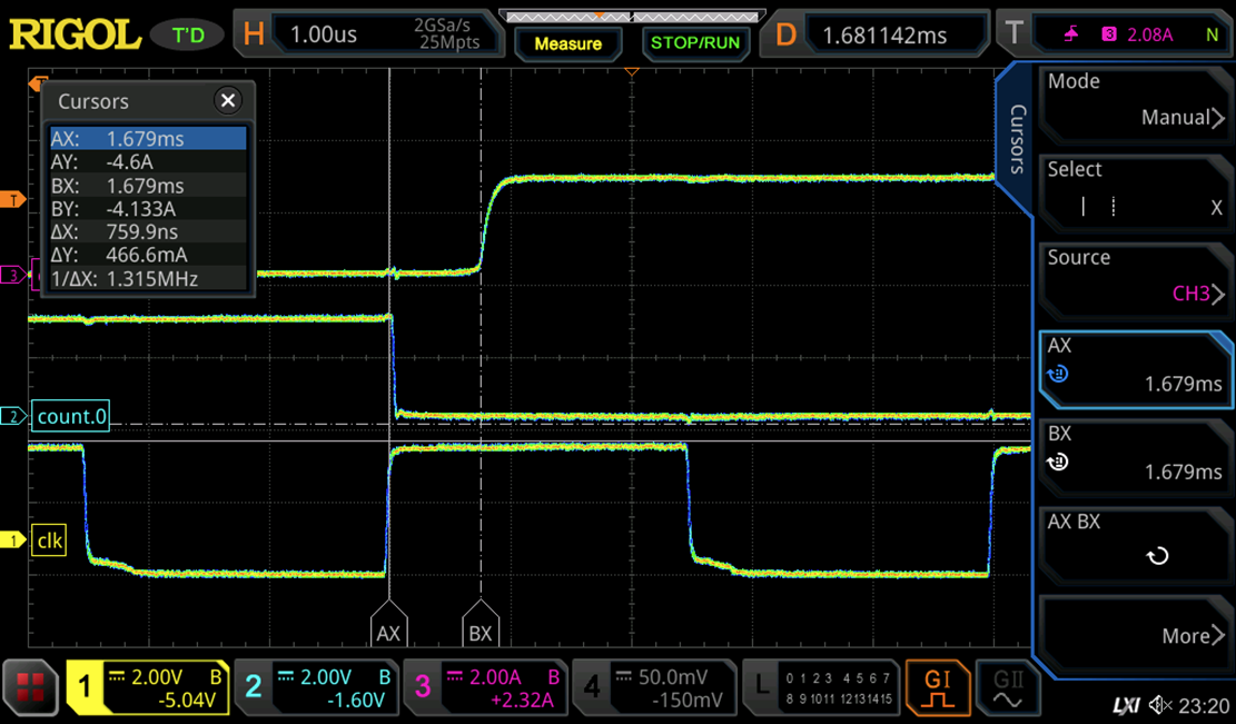 The timing bevavior of the pass gate latches is a bit different than that of the polarity hold latches. Now we only have a single inverter going from the clocked pass gate to the output. This means that the timing becomes dependent on the input data. The L->H transition on the output is delayed by 750ns. The reason for this is twofold: First we observe the storage time of the output inverter, secondly the pass gate transistor is operated in inverse direction (Emitter and Collector are swapped) where the hfe is much lower. I may have to ponder a bit how to improve this. Maximum clock speed is around 450kHz, a bit slower than the 15T DFF.
Summary
All in all this is a big succes. The flow delivered perfectly working PCBs on the first attempt! Next step is to play a bit with logic styles to opimize size (cost) and speed.
Discussions
Become a Hackaday.io Member
Create an account to leave a comment. Already have an account? Log In.