hesam.moshiri
DC to DC converters are quite popular among electronic enthusiasts and are widely used within the industry. There are three major types of non-isolated DC to DC converters: buck, boost, and buck-boost. In this article/video, I used there major components such as the famous UC3843 chip, a power Schottky diode, and an N-Channel Mosfet to design a compact DC to DC boost converter. The input voltage could be as low as 9V that makes it suitable for a variety of applications, such as 12V to 18V conversion to power a laptop computer using a single 12V battery.
I used Altium Designer 21 and SamacSys component libraries to design the schematic and PCB. The PCBs have been fabricated by the PCBWay in the green solder mask. Also, I examined the noise figure of the circuit using the Siglent SDS2102X Plus/SDS1104X-E oscilloscope and Siglent SDM3045X multimeter. So let’s get started!
Specifications
Input Voltage: 9-16V
Output Voltage: 28Vmax (can be increased, see the text)
Output Current: 4Amax
Output noise (no load): 5mVrms
Output noise (2A load): 27mVrms
A. Circuit Analysis
Figure 1 shows the schematic diagram of the DC to DC boost converter. As it is clear, the heart of the circuit is the UC3843 chip [1].

Figure, Schematic diagram of the UC3843 DC to DC boost converter
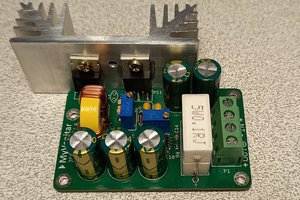
C1 and C2 have been used to reduce the input noises. L1, D1, and Q1 build a boost conversion network. L1 is an 8A to 10A 100uH inductor. D1 is the MBR20100CT [2] Schottky diode (two parallel diodes in one package). Q1 is the IRFZ44 N-Channel Mosfets [3]. The ON resistance (RDS(ON)) of the Mosfet is just around 28 milliohm and it can handle up to 50A at 25C. So, these characteristics make these components a good fit for this project.
IC1 is the controller of the boost converter circuit. According to the UC3943 datasheet: “The UC3842/UC3843/UC3844/UC3845 are fixed frequency current-mode PWM controller. They are specially designed for Off-Line and DC to DC converter applications with minimum external components. These integrated circuits feature a trimmed oscillator for precise duty cycle control, a temperature compensated reference, a high gain error amplifier, a current sensing comparator, and a high current totem-pole output for driving a Power MOSFET.”
C3, C4, C5, C6, and C7 are used to reduce the output noise. Usually, a boost converter output is noisier than a buck converter, especially by using discrete components. A single-chip buck/boost controller is less noisy, however, the output voltage and current of these controllers are limited.
R1 is a 10K multiturn potentiometer that you can set to adjust the output voltage. You can increase the output voltage level by decreasing the R5 value. The output voltage is determined using this formula:
Vout = 2.5 (1 + R1/R5)
So as it is clear when R5 is 1K, then the maximum output voltage is somewhere between 27V to 28V. if we decrease the R5 value to 820R or 680R, then the maximum output voltage would be around 32V to 33V or 39V to 40V. I don’t recommend increasing the output voltage more than this because the voltage + noise level might cross the rated voltages tolerances of the capacitors (50V), which of course might be lower than 50V in practice (due to manufacturing tolerances). R2 and R3 have been placed in parallel that builds a preliminary load to help to stabilize the output voltage.
B. PCB Layout
Figure 2 shows the PCB layout of the design. It is a two layers PCB board with a mixture of SMD and through-hole components. A view from the top layer, bottom layer, and silkscreen and solder mask (top layer) have been all included in figure 2.

Figure, The PCB layout of the DC to DC boost converter
As I mentioned in the abstract, I used the Altium Designer software [4] to design the schematic and PCB. I did not have the schematic symbol, PCB footprint, and 3D model of several components in this project. So instead of wasting my time in designing the component...
Read more »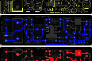
 ElectronicABC