 Ken Yap
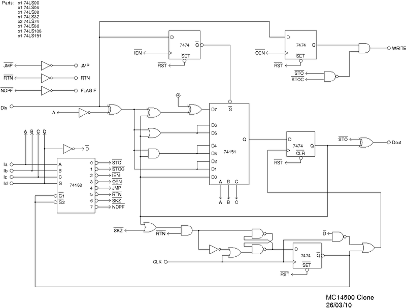
First thing is to see what has been done before. In the project #One Bit CPUs a previous design in TTL is mentioned and the diagram is here.
It makes sense to elaborate the design modularly, so let's first look at instruction processing. You'll notice that the 16 instructions fall into two groups when you exclude the NOPs at 0 and F. The first 7 are load and logical operations. while the next 7 are store and control operations. The difference is that only the former affect the result register (RR). So I'll adopt the design and create a logic unit LU (no arithmetic, so not ALU). This is done using gates and an 8 input multiplexer feeding a D flip-flop which is the RR.
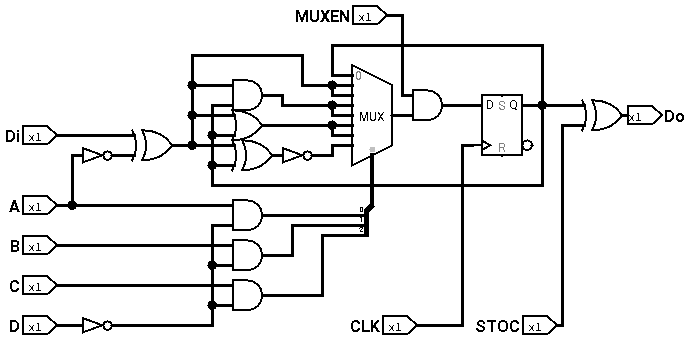
In order from 0, the operations are NOPO, LD, LDC, AND, ANDC, OR, ORC and XNOR. The first is just the identity transform, so RR out is looped back to RR in. At this point I have to gripe about the ordering of the operations as designed. LD is 1 and LDC is 2. It would have been nice if XNOR had been moved to 1, then LD and LDC would be 2 and 3 respectively, thus differing in only one bit. Similarly for AND and OR. Fortunately this doesn't complicate the circuit because of the multiplexer, we just use A to invert the Di as necessary.
The instruction line D is used to force the operation to NOPO using 3 AND gates so that the RR is unchanged by the top 8 instructions. In the original design this was done by futzing with the clock signal. I believe this is a mistake because it can lead to glitches.
If you have been following the project, you may notice that the circuit has been updated to be modular, see this log.
Discussions
Become a Hackaday.io Member
Create an account to leave a comment. Already have an account? Log In.