Close
0%
0%

Modular differential probe

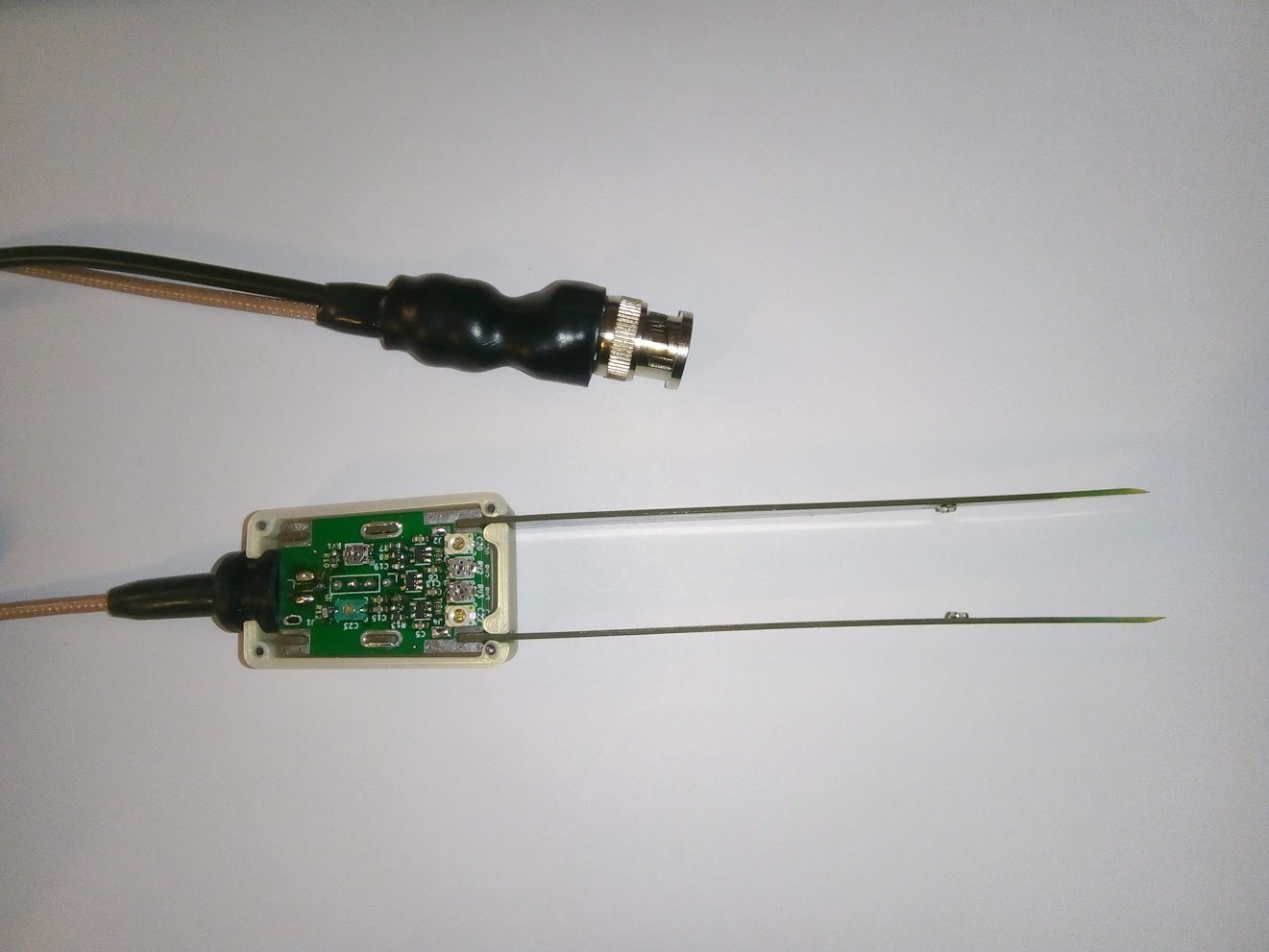
100 MHz differential probe for oscilloscopes, with modular accessories to suit both high and low voltage use.

Public Chat
Similar projects worth following
Oscilloscope is the most important instrument for studying modern high-speed circuits. Entry-level oscilloscopes are affordable, but they come with passive probes only. These affect the behavior of the circuit being measured and can only measure voltages against reference ground. Active differential probes are much more versatile.

Low-cost differential probes currently on market focus mainly on high voltage use, and have clumsy large attachments that are unsuitable for measuring small parts. More advanced probes cost thousands of dollars and go to gigahertz bandwidths, which is unnecessary for many purposes.

This project aims to create a differential probe with target price of 100-200 USD. It will have switchable accessories that allow different voltage ranges and connection styles. The accessories have been designed to minimize capacitive loading of circuits.

Schematic & basic structure

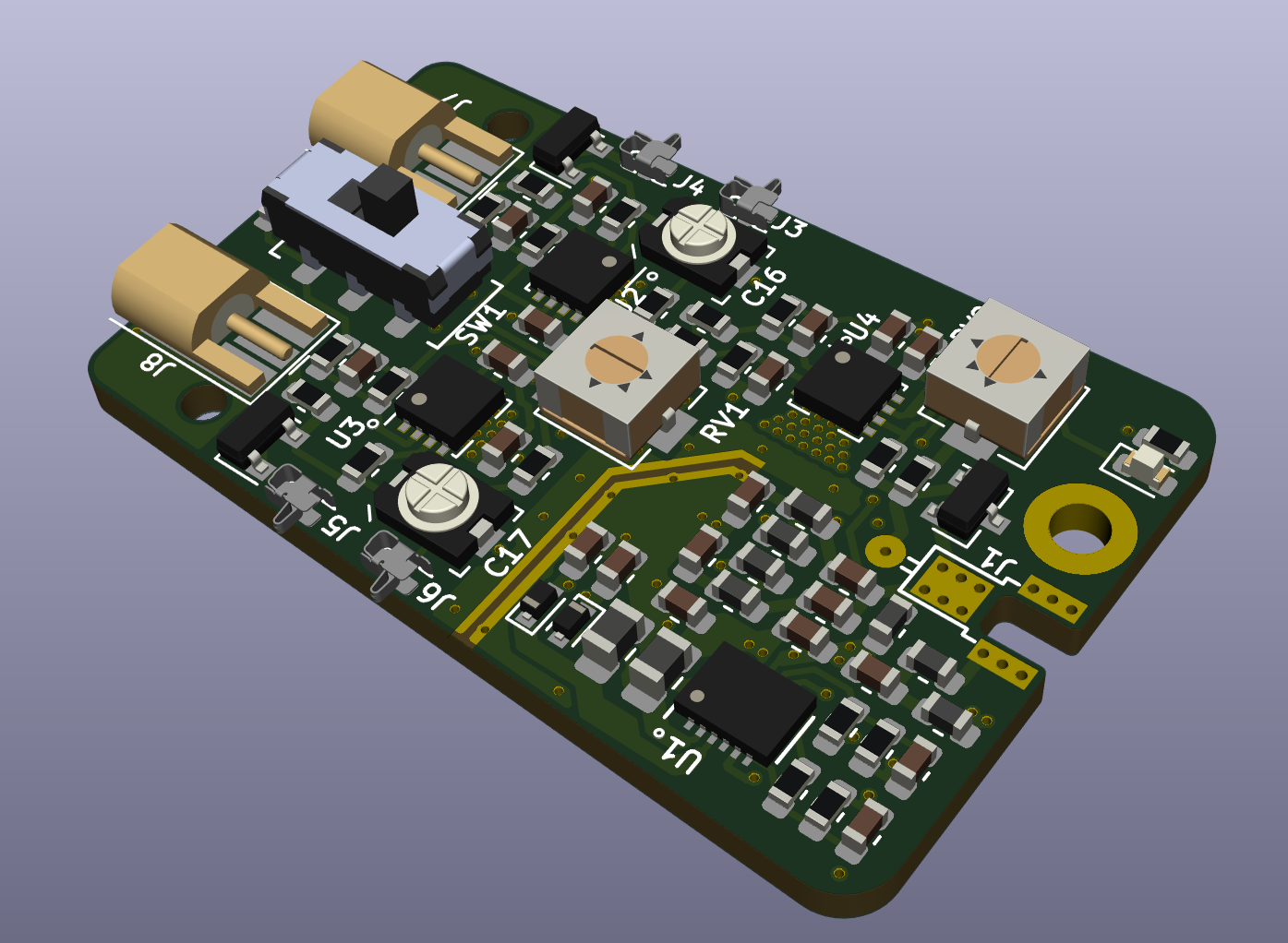
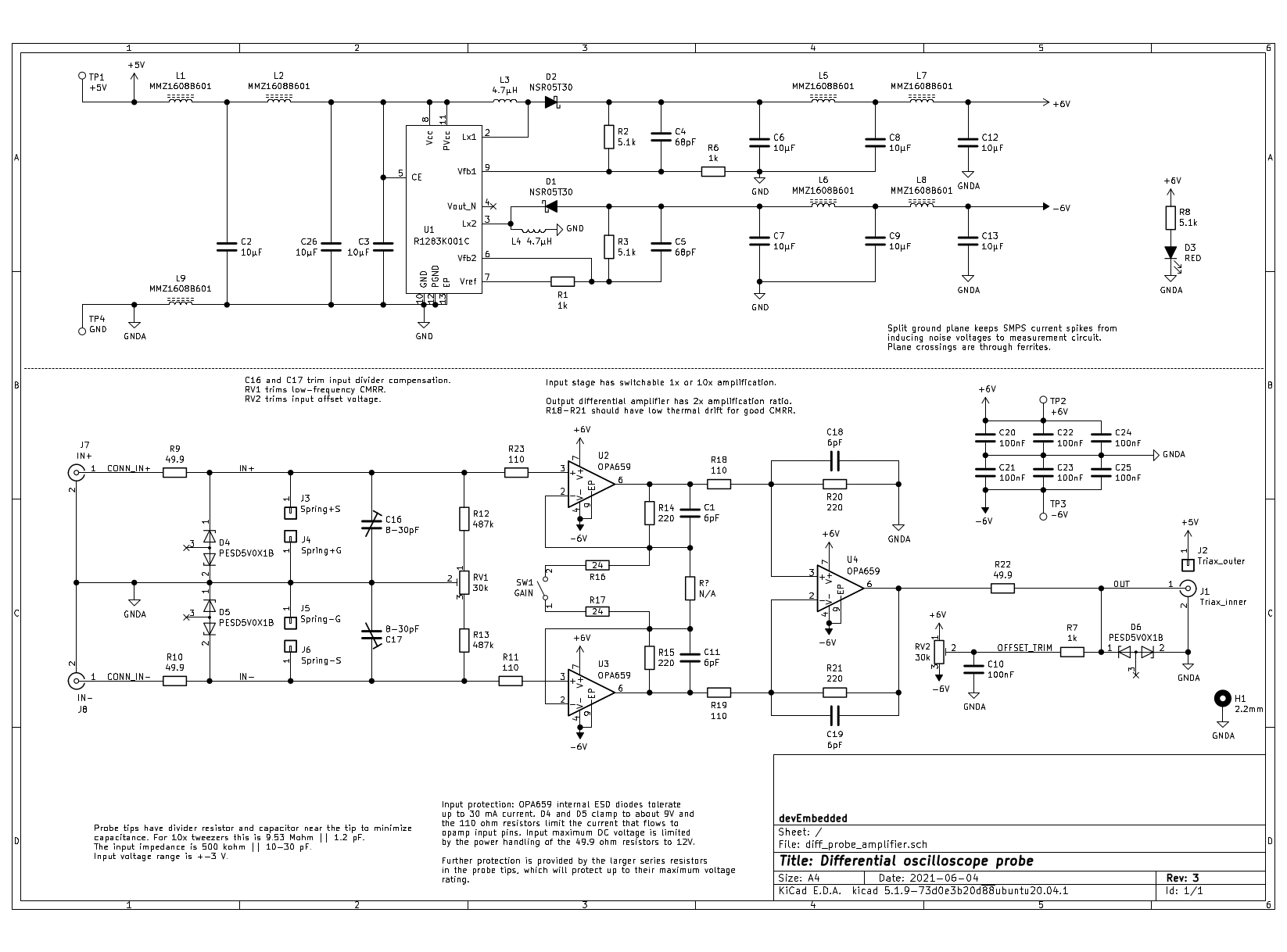
The amplifier PCB consists of a +- 6V power supply, and a differential amplifier made of three OPA659 opamps. The power supply section is based on R1283 DC-DC converter. It has two stages of LC filtering on output to minimize the output noise. The operational amplifiers are arranged in traditional instrumentation amplifier topology.

The input impedance is nominally 500 kilo-ohms and 20 pF. Because different accessories will vary in their exact component values, the input stage is made adjustable with trimmer capacitors and resistors. These will need readjustment when accessory is changed, but the procedure is fairly simple (see user manual).
Frequency response

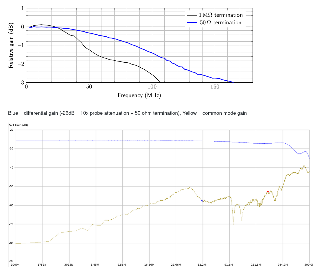
The two common termination impedances used in oscilloscopes are 50 ohm and 1 megaohm.  Of these, 50 ohm termination is generally preferred for active probes because it is easier to get flat frequency response with it. By providing 50 ohm series termination at the source side, the probe works reasonably well with 1 Mohm termination also.

Preliminary frequency response curves have been measured with NanoVNA V2 and with Rigol DS1054Z scope, both give similar results. The response is still being tuned, especially to improve CMRR at high frequencies.
Accessory attachment

The tweezer tips attach using a taper lock mechanism against the plastic case. Small spring contacts provide the connection between main PCB and the tips.

For cable accessories, coaxial connectors are used. MCX and MMCX have been tried, MMCX is a bit smaller and will probably be chosen for the final version.

Current plans include tweezer tips for probing IC pins, 60 V accessory that connects to pin headers / grabber hooks, and 600 V CAT II accessory with banana plugs. Perhaps a shunt resistor accessory also to easily measure currents.

To minimize input capacitance, the accessories have the divider resistor & capacitor as close to the measurement point as possible. A coaxial cable will connect them to the main amplifier, shielding the signal against ambient noise.


  • 1 × Differential amplifier PCB Including 3x OPA659, 1x R1283 and various other SMD parts.
  • 2 × Plastic enclosure The enclosure consists of two identical halves.
  • 1 × Triaxial cable assembly Supplies +5V power from oscilloscope USB connector, and passes signal to BNC connector.
  • 2 × Tweezer tip PCB Gold plated PCB with a few passive components.
  • 2 × Cable to square pin accessory Tiny PCB with resistor, capacitor and pin socket, and cable to MMCX connector.

View all 6 components

  • Enclosure molding

    Petteri Aimonen10/12/2021 at 07:26 0 comments

    My initial plan for the enclosure was just to order it 3D printed. Even home printed enclosures look nice enough, and commercial printers like HP Multijet Fusion give very nice looking results for affordable prices. The cost for the complete enclosure printed in HP MJF PA12 material is about 6 EUR in 10 pcs quantities. Very good.

    But then in spring 2021 I hit an issue with another project of mine: HP MJF PA12 is only fire rated to UL94 HB. The IEC 61010-1 safety standard for measurement instruments requires enclosures to have a rating of UL94 V-1 or better.

    There is an available 3D printing material PA2210FR with the required rating, and in spring the price seemed acceptable at around 12 EUR per enclosure. But now the price has ballooned to 30 EUR per enclosure, which is way too much for the price point I'm aiming for.

    An alternative would be to either use a standard off-the-shelf enclosure, or just sell this without complying with the CE mark requirements. I do not want to do either of these.

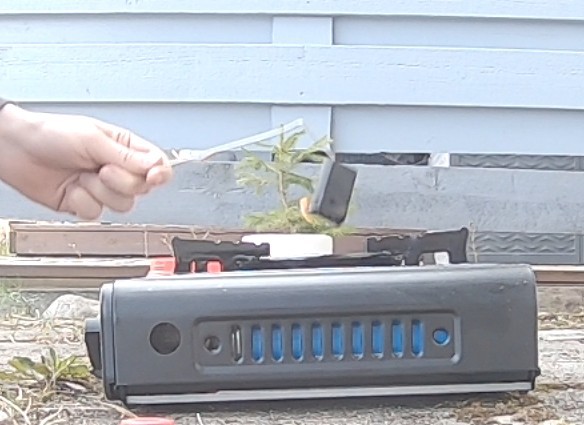
    I did some home tests for HP MJF PA12 material, and it appears that at 2 mm thickness it does meet the UL94 V-1 requirements, but my home tests are pretty unreliable and proper testing would cost more than I want to spend at this point.

    For bigger volumes, the vacuum casting offered by PCBWay is an option also, but at 10 pcs quantities the quote I received was 40 EUR per enclosure.

    So, time for plan B: silicone molds. Years ago I read Michal Zalewski's excellent Guerrilla guide to CNC machining, mold making, and resin casting. I've wanted to try it out as soon I just had some project that would benefit. I even built a vacuum pump and chamber out of an old fridge compressor and cooking pot a few years back, but didn't go further than that.

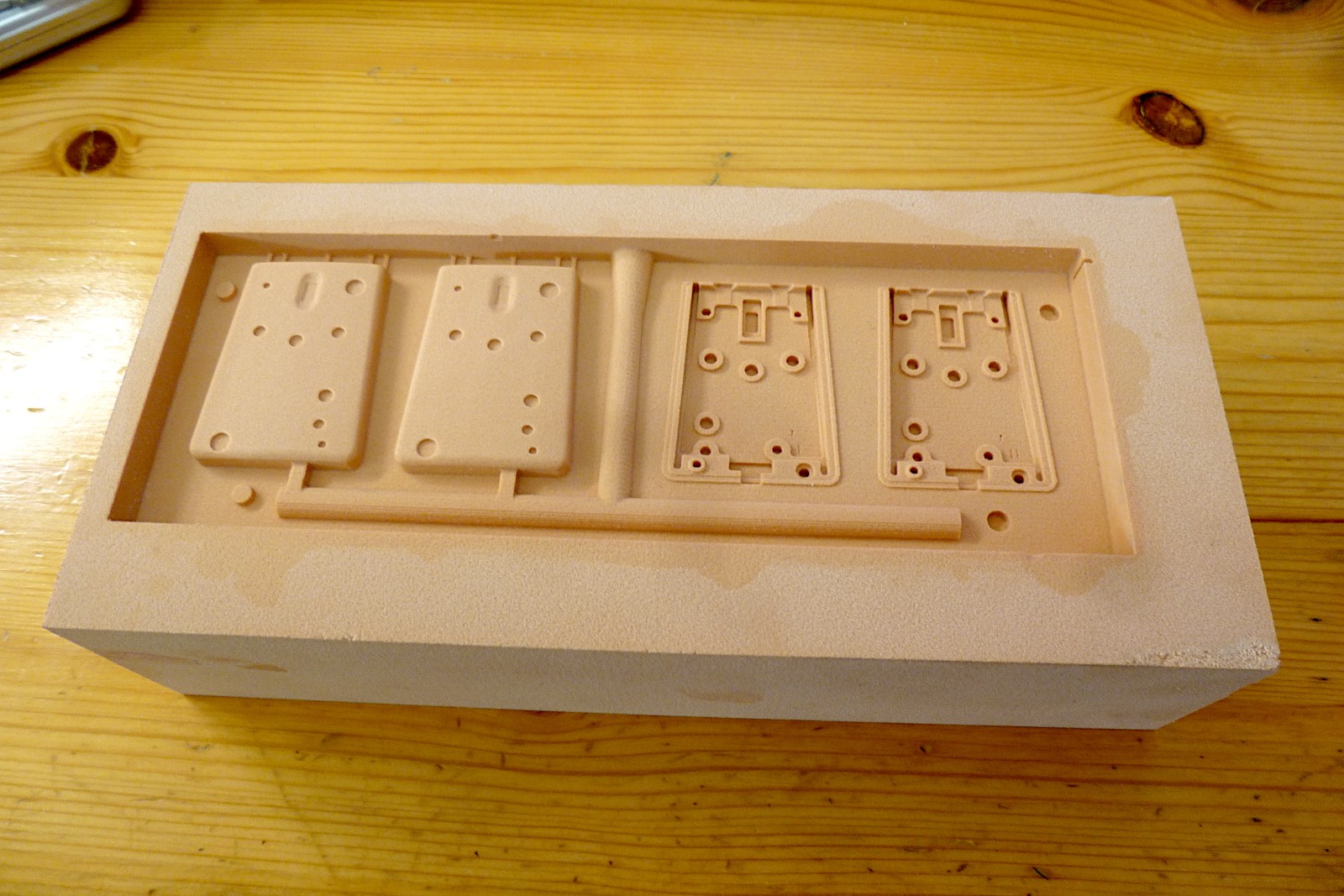
    I've followed the guide quite closely. I made the mold using my CNC3020 out of SikaBlock M450 modelling board, bought from Modulor. It was a joy to machine, but has a slightly porous surface. I'm going to try some spray lacquer to make it smoother. I designed the "mold mold" so that I could cast two identical silicon molds out of that, and those placed together would yield the final part.

    My part is not the easiest to cast because it requires a two-part mold and has quite intricate details that can easily trap air. The flame resistant TASK 7 resin I'm using also has a very short pot-life of 2.5 minutes. In my first tests, it started to harden before it could flow through to the upper parts of the molds.

    I then switched to vacuum casting: the cooking pot lid has a convenient hole that I can pass a 5mm silicon hose through and into the round channel in the silicon mold. I clamp the hose shut while drawing vacuum to the pot. As soon as the resin is mixed, I put the end of the hose in the mixing jar and carefully let the vacuum draw the resin into the mold. One just has to be careful to keep the end of the hose submerged, otherwise air gets drawn in also.

    As soon as the resin starts coming out of the air holes at the top, I let air into the vacuum chamber. This collapses any remaining low-pressure air bubbles to about 5% of their original size.

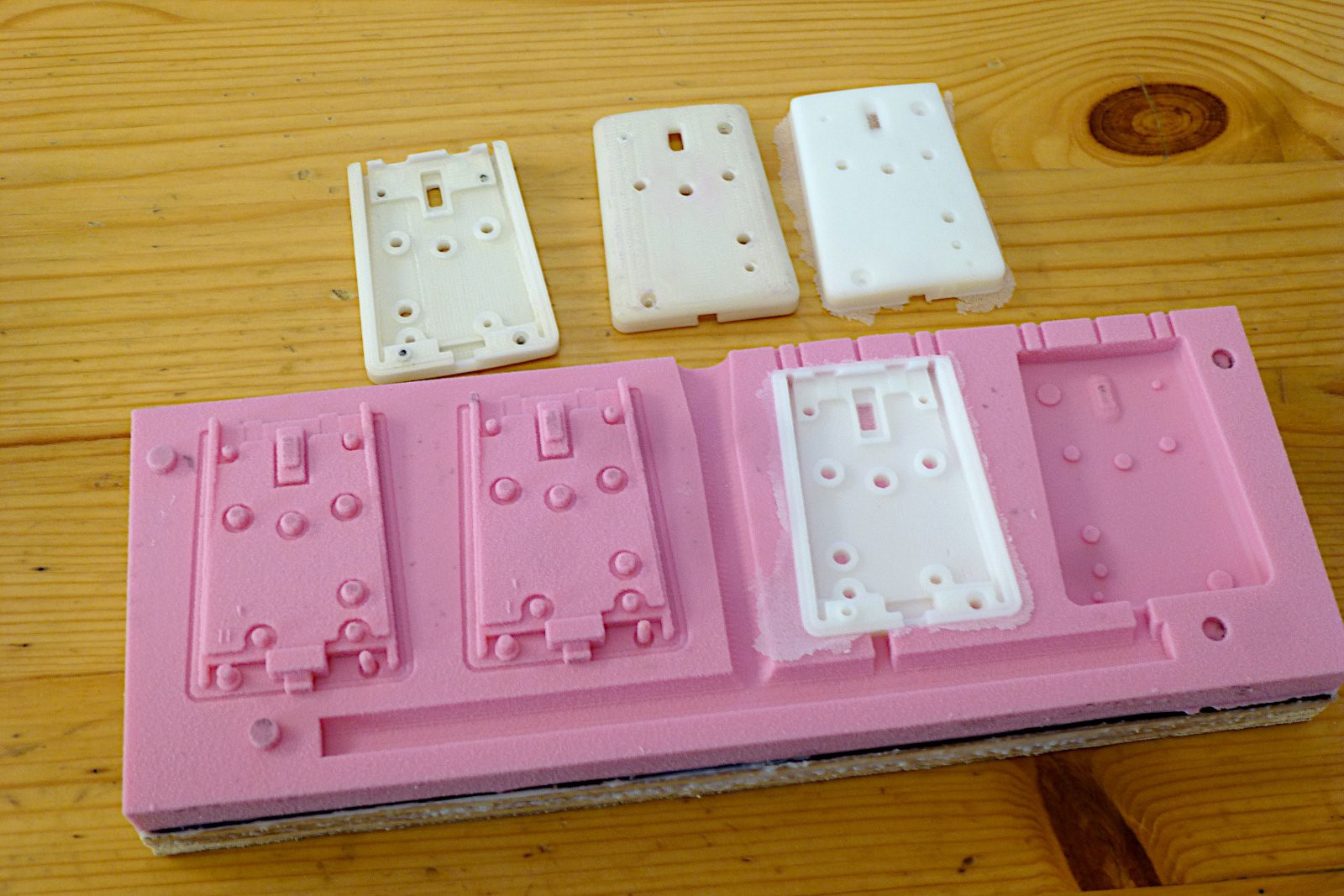
    Above is two enclosure halves printed on Prusa i3 MK3S, and two made with vacuum casting. The surface is very nice, but I still need to work on the mold design to reduce the amount of cleaning needed. The dimensional accuracy is also better than 3D printing, so I can reduce the tolerances a bit for a better fit.

  • First impressions of rev 4 prototype

    Petteri Aimonen09/06/2021 at 08:22 0 comments

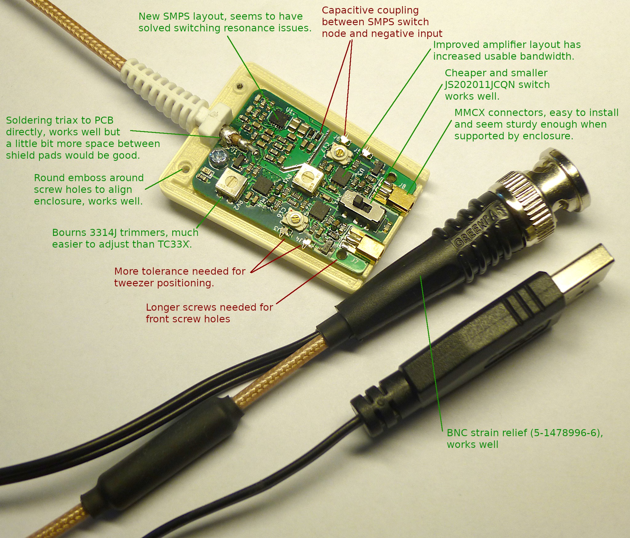
    I received the revision 4 PCBs last week and have assembled one prototype. I already hoped that I wouldn't find anything more to improve, but that doesn't seem to be the case. Normally at this point a boss would say "it's good enough, wrap it up" - but my current boss (myself) is very bad at knowing when to stop.

    Biggest letdown is the return of SMPS noise. Not conducted noise, mind you, but capacitively coupled noise. In relayouting the SMPS section and adjusting the frontend layout, I ended up moving the negative input spring terminal too close to the switching node of the SMPS. This causes a few mV amplitude square wave to appear, especially when probes are floating. The fix should be simple enough, moving the parts around a bit so that the capacitors will better shield the terminal. Though there is an alternative of just installing a bit of copper tape as a shield manually.

    When ordering the PCBs, I had to make a last minute change to the design because the parts next to MMCX connector were too narrow to manufacture. As a consequence, the front screws now go all the way through the PCB, and the 8 mm long screws do not have enough plastic to hold well. It will be a simple matter of switching to 10 mm screws and adjusting the enclosure design to have through holes for them.

    Finally, for some reason, I seem to have even worse tolerance for the tweezer tip fitting in the 3D printed enclosure than before. But thanks to the PCB change, there is now much more space for the ground spring contact up front, so it would be possible to adjust the layout to make it more tolerant of enclosure inaccuracies.

    Overall, I think my perfectionism will require a revision 5. But the changes are getting smaller, so hopefully if I test this prototype well, the next version is something I can call "final" and start manufacturing.

  • Power supply filtering

    Petteri Aimonen08/26/2021 at 07:24 2 comments

    In the comments of the Hackaday post about this project, a question was asked why I chose to use ferrites instead of a linear regulator for filtering the output of the SMPS.

    The short answer is: Because linear regulators do not do much filtering above 10 MHz. But I realized that I've never actually verified that assumption, so I decided to do some tests.

    On what frequency is the noise?

    First of all, what does the noise at the output of the 1.4 MHz SMPS look like? Is the ripple mostly at the 1.4 MHz fundamental frequency, or is it higher?

    The SMPS output capacitor is 10 µF nominal, which is actually about 5 µF due to effects of DC bias. The load current is 90 mA. Calculating from this, we can expect a fundamental frequency ripple of about 13 mV before any filtering. Scope measurements confirm this.

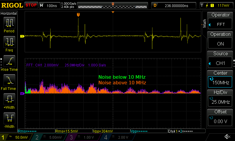
    But there is up to ±200 mV switching spikes that have much higher frequencies:

    By doing a FFT analysis and setting both frequency and vertical axis to linear mode, we can estimate the amount of total noise in frequency bands by looking at the area under the curve. As seen above, the noise is quite wideband and evenly distributed up to 150 MHz (at which point the scope bandwidth starts to limit sensitivity). Because the area above 10 MHz is much wider than the area below 10 MHz, the high frequency noise contributes most of the total noise amplitude. Furthermore, the operational amplifier is more sensitive to power supply noise at higher frequencies - OPA659 itself has a PSRR of 55 dB at 1.4 MHz, but only 15 dB at 100 MHz.

    How well do LDOs block high frequency noise?

    Most common linear regulators are only rated up to 1 MHz, but there are high-PSRR models that have ratings up to 10 MHz. For this test, I am using TPS7A2030 regulator, which has specified PSRR of 50 dB up to 10 MHz. How well does it block noise above this frequency?

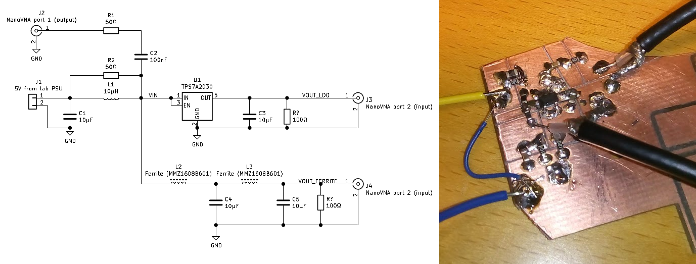
    I made a quick test circuit, where NanoVNA feeds a high frequency signal through C2 to the input, while DC current flows through L1. A small problem in the measurement is that I couldn't add any kind of input filter capacitor, as NanoVNA wouldn't be strong enough to drive a strong ripple into it. L1 isolates the input capacitor for high frequencies, so that NanoVNA is able to make about 20 mV ripple at the input of the regulator. I calibrated NanoVNA v2 against the VIN point, i.e. any losses in R1 and C2 should be cancelled.

    (Note: I'm using the NanoVNA v2 that has DC blocking capacitors integrated. If your VNA does not, check the maximum voltage rating and add a series capacitor if needed.)

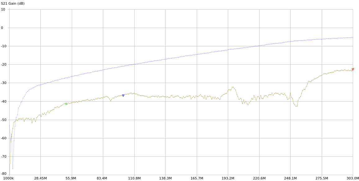
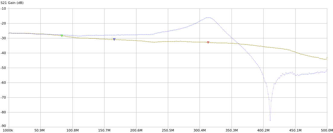
    Here are the results. Blue curve is VOUT_LDO and yellow curve is VOUT_FERRITE:

    As expected, LDO does a very good job of filtering out low frequency noise. Because of the loading and noise level of the VNA, the measurements at 1 to 5 MHz fluctuate a bit, but the blue LDO curve is generally lower there. For some reason I'm not quite achieving the specified 50 dB PSRR for the regulator at 10 MHz, so there may be some defiencies in my measurement setup.

    But in general, this seems to support my assumption that a ferrite + capacitor filter will do a better job of filtering at the high frequencies that are of importance here.

    But that was the easy part

    In reality, filtering out the noise that gets conducted directly through the output power rails is the easy part. The difficult part is inductive and capacitive coupling, which gets quite strong when the distance between the SMPS and the amplifiers is only 15 mm.

    Basic methods to reduce this is to use shielded inductors and to keep the SMPS layout as compact as possible. The largest current spikes are on the input side of the SMPS, so that needs filtering also. Adding shielding around the SMPS section can help also, but it complicates manufacturing so I would like to avoid it if possible. A synchronous rectification SMPS chip would typically reduce noise also, but I haven't found a suitable one for dual-sided ±6V power rails.

    ... Read more »

  • Revision 4 PCBs ordered

    Petteri Aimonen08/23/2021 at 06:56 0 comments

    I've finished the design for revision 4 PCBs. The schematic changes at this point are quite minimal, but it was still a complete redesign of the PCB layout.

    The largest change is switching to MMCX connectors for cable inputs. They appear to be better available in surface mount versions than MCX, and they are also significantly smaller. This in turn allowed placing the gain selector switch between the connectors, which made it possible to make the layout more symmetric and relocate other parts closer to the front-end amplifier. All high-speed signals now stay on top layer, which might further improve the high frequency response.

    The spring contacts for the tweezer tips are now positioned at 5 mm distance instead of the previous 2 mm. This gives more leeway for inaccuracies in the plastic enclosure. The tweezer tip PCBs now have gold plated contact pads on both sides, so they can also be inserted facing outwards - this could be useful for measuring through-hole parts or some connectors.

    I've switched the trimmer potentiometer to a larger and more robust Bourns 3314 type. The trimmer capacitor footprint has been modified to fit both Knowles JZ200 and JR200 types, which have lower thermal drift than the previous SGC3S300.

    Revision 3 introduced a bit of resonance problem in SMPS section after I had thoughtlessly moved the ground plane under it from layer 2 to layer 3, increasing the ground plane distance from 0.2 mm to about 0.8 mm.  Now the ground plane is back where it belongs and the SMPS layout has been made tighter also. I'll also switch the SMPS diodes to a lower capacitance version.

    The power led is now connected to -6V rail, so it will not light if the SMPS is not operating (such as due to low voltage or over current cutoff). Because of the boost topology, +6V rail gets +5V from input even when SMPS is stopped.

    Based on revision 3 tests, split ground plane for the SMPS section is beneficial in this circuit. I've however added a pair of tracks that can be soldered together to solidly connect the ground planes, so that I can better test the noise levels.

    Previous versions (ab)used brass standoffs for soldering in the triax cable. That worked well, but the change to MMCX connectors moved the centerline of the board too low for that solution. Instead, a small slot is now made in the PCB edge for soldering in the triax.

  • Lots of ferrites

    Petteri Aimonen08/18/2021 at 11:07 0 comments

    Every time a point in circuit has both inductance and capacitance without enough damping resistance, there will be a resonance. A common design approach is to try and keep these resonance frequencies away from the signal frequencies you are interested in. But with a wide band design, such as this probe, it is often not possible.

    Simplest way to damp resonances is to add a resistor. I've found Okawa RLC design tools especially helpful in quickly trying out different values. But resistors are not frequency selective, so they always affect the normal function of the circuit.

    An alternative is to use ferrites, which are lossy inductors. Their frequency response depends on the material used: some are effective starting at 1 MHz, others only above 100 MHz. This allows careful selection to dampen at the resonant frequencies without affecting the signal frequencies too much.

    So far I have three main uses for ferrites in this design: power supply filtering, input resonance dampening and common mode resonance dampening.

    Power supply filtering

    The amplifier circuit requires two-sided supply, in this case ± 6 V. This is generated from +5 V using a 1.4 MHz switching mode boost converter, which necessarily causes some ripple when it switches.

    The ± 6 V rails are filtered with two stages of series ferrites and parallel capacitors. Because the fundamental frequency is low, I chose the lowest frequency ferrites I could find, specifically MMZ1608B601, combined with 10 µF ceramic capacitors. These do a fairly good job of filtering out the low frequency ripple and very good job of filtering out the high frequency harmonics. This is important because the opamp power supply rejection ratio gets lower as frequency increases.

    But filtering the SMPS output is not enough. The +5 V input goes alongside the signal cable, and usually comes from the same oscilloscope that is doing the measuring. Large current spikes on input supply could couple into the output signal. To avoid this, also the input has two stages of ferrite filtering. But because the input current is twice as high as the output current of each rail, a ferrite with higher saturation current is needed, specifically BLM18KG102. Input from cable goes directly to first ferrite - if there was an initial filter capacitor, it would minimize voltage noise but could cause current noise when connected to a noisy power supply.

    Finally, after a bunch of testing, I ended up using a split ground plane for the SMPS portion of the PCB. The power and signal grounds are connected together with a ferrite, and last stage of ± 6 V filtering is against the signal ground. This seems to minimize the noise spikes that get coupled to the amplifier, though I'm not entirely sure of what kind of coupling is at play here.

    Input resonance dampening

    The input cables have their own inductance, which forms a resonance when combined with the input capacitance. This can be reduced by keeping the cables as short as possible and close together, but practical considerations often get in the way.

    A common trick is to add a series resistor to dampen the resonance. This forms a low-pass circuit, which causes the frequency response to droop at much lower frequencies also.

    An alternative is to add a ferrite ring around each of the input cables. Because of the frequency selectivity of ferrites, this often has less effect on the lower signal frequencies.

    Above, 2x 15 cm input cables are measured. Blue curve has a 50 ohm series resistor, while yellow curve has both a resistor and a ferrite.


    Common mode resonance dampening

    Similarly to input cables, the output cable between oscilloscope and the amplifier has inductance. Because it is longer, the inductance is higher and the resonance peak ends up lower, at about 40 MHz. The coaxial cable acts as a transmission line, so the inductance does not directly affect the output signal, but it does affect the potential difference between oscilloscope ground and the amplifier ground, i.e. the common...

    Read more »

  • ESD protection

    Petteri Aimonen08/06/2021 at 13:12 0 comments

    Designing ESD protection for measurement circuits is often difficult. Parasitic capacitance and leakage currents must be minimized so that the signals are not distorted.

    As a complete unit, the differential probe is already quite well protected: the 9 megaohm resistors in the input divider will limit ESD pulses to very low currents, low enough that the integrated protection diodes in OPA659 can absorb them. To add extra protection for when cables are being attached, ESD diodes can be added to the inputs. PESD5V0X1BT is probably a good option, as it has relatively low clamping voltage but also low leakage current and capacitance. PESD4V0Y1BSF would be even better, but its 0201 package is getting too small for me to reliably assemble.

    That takes care of the amplifier protection.

    But do the cables themselves need protection? After all there is a small ceramic capacitor and SMD resistor in each accessory, which could get damaged by a current pulse. Finding a suitable ESD diode for this proved difficult, as most 60 volt ESD diodes have both large capacitance and large leakage currents.

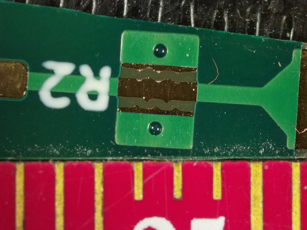
    One alternative is to use a PCB spark gap as rudimentary protection. I got some boards made, and a 0.2 mm gap arcs over at 800 volts. I still need to finish my ESD tester to find out if there remains risk of damage to the probe assemblies.

  • June 2021: In search of the perfect pin socket

    Petteri Aimonen08/06/2021 at 13:03 0 comments

    2.54 mm pitch pin headers with 0.6 mm square pins are pretty much the de-facto prototyping connector for all low voltage uses. Many grabber hooks and cables are designed to fit this. But there is considerable variation: sometimes the 0.6 mm pins are instead round or U-shaped. And usually the cable-mounted so called "DuPont connectors" do not last very long before they start making a poor connection. I certainly don't want to ruin the probe usability by having a flaky accessory.

    Because I want to minimize the probe capacitance, there is the extra complication that the pin socket connector must be mounted on a small PCB with 0603 resistor and capacitor on it. That then gets soldered to the end of a coaxial cable and heatshrinked - and it should still fit between 2.54 mm pitch pins!

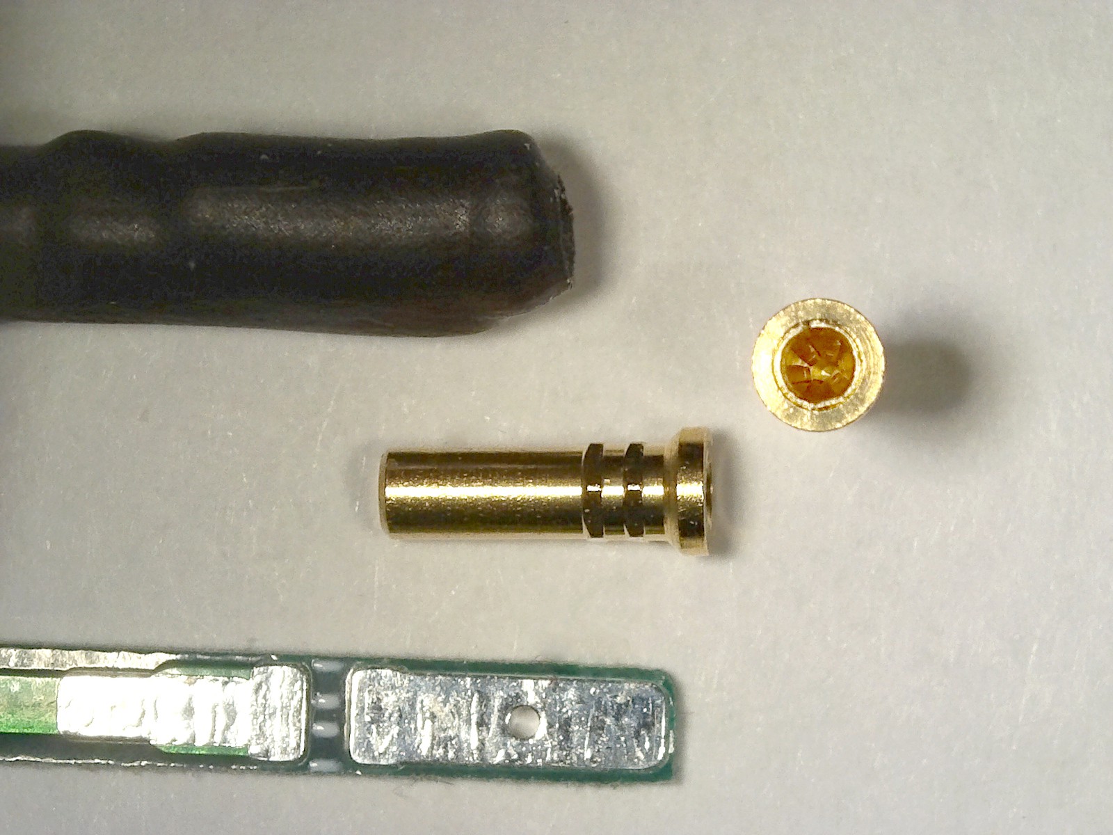
    After a bit of searching, I found Mill-Max 0279-0-15-15-47-27-10-0 sockets. They are tiny, yet have real gold-plated six-sided spring mechanism inside. This should last much longer than the tin-plated one-sided springs.

    Best of all, it fits on a tiny PCB and the width is 2.3 mm with a single layer of heatshrink applied. Because the shaft has hex-shaped protrusions, it should work in a reflow process also - at least if placed manually.

  • May 2021: Revision 2 prototype

    Petteri Aimonen08/06/2021 at 12:30 0 comments

    The second revision prototype switched to OPA659 for larger bandwidth. The tweezer tips are now attached using small spring contacts. The tip PCBs have a taper shape that will lock in place when pushed against the enclosure.

    This version also added a gain switch to select between 2x and 20x amplification. The 2x output stage gain is always included because it extends the common mode voltage range of the input, while the input stage can have either 1x or 10x gain.

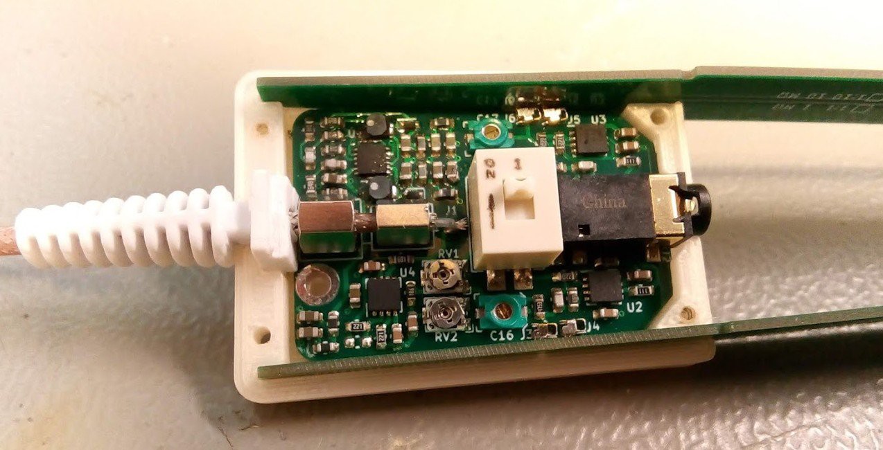
    The initial plan was to use a 3.5 mm jack with shielded cable for the probe accessories. The input impedance is 500 kohm, so matching it with a coaxial cable is not possible - and the cables can be kept short enough to not need matching anyway. The common audio cables seemed a reasonable low-cost option, but it turns out PVC insulation in them has a huge variance in capacitance. It varies both by frequency and by temperature, making it impossible to properly compensate the inputs. Real coax connectors will be needed.

    Otherwise the second prototype works well and has a bandwidth of over 100 MHz. There is a bit of noise issues, and some thermal drift on startup. These can probably be improved by adjusting the PCB layout.

  • February 2021: First prototype with OPA810

    Petteri Aimonen08/06/2021 at 12:22 0 comments

    First prototype was based on OPA810 amplifier and +-12V supply voltage. The tweezer tips were permanently attached by soldering:

    It was very promising, though the bandwidth was limited to about 50 MHz. However, it was clear that tweezer tips are mostly useful for probing between IC pins, and other uses would need different accessories.

    Initial plan was to try to push the cost as low as possible, to around $50 USD sale price. However this would limit the performance a lot. Instead it seems better to have more versatility by having accessories for different voltage ranges and purposes - one amplifier can be extended with cheap attachments.

    Switchable accessories will require readjustment of the compensation & CMRR trimmers, but that should be a quite fast process using e.g. the calibration output available on most oscilloscopes.

View all 9 project logs

Enjoy this project?

Share

Discussions

Michael LaVigne wrote 10/01/2021 at 20:45 point

Got everything hooked up and had some slew rate issues so i changed the probe capacitors to 4.5pF and the waveform is perfect now!  Epic, cant wait to test this with the VFD running to see how it handles the noise!

  Are you sure? yes | no

Petteri Aimonen wrote 10/02/2021 at 05:29 point

Very nice! For optimum bandwidth C1, C11, C18 and C19 may need some tuning also for different layout / opamp type, though I think 6 pF probably gets close to maximum performance of OPA810.

  Are you sure? yes | no

Michael LaVigne wrote 08/30/2021 at 21:01 point

Awesome project- I would love to build one.  Where are you finding stock of the OPA659 opamp?  TI is showing it out of stock everywhere.

  Are you sure? yes | no

Petteri Aimonen wrote 08/31/2021 at 04:04 point

Yeah, I bought the last ones a few weeks back. So I have 20 for protos, but hopefully it will get back in stock eventually.

I'm not sure if there is any viable alternatives for the same bandwidth, but OPA810 works up to 50 MHz. It needs a different footprint & the +-6V supply can be raised to +-10V.

  Are you sure? yes | no

Michael LaVigne wrote 08/31/2021 at 20:26 point

Awesome, thanks for your help.  I reworked it to accept the OPA810 with the SOT23-5 footprint (which fits without too much rework and also is an optional footprint for the original OPA659) and left the supply at +/-6V.  This is my first 4 layer board (and high frequency circuit) i've messed with, so fingers crossed!  Thankfully my application is relatively slow RS485 comms, so it shouldn't matter too much.

  Are you sure? yes | no

Petteri Aimonen wrote 09/01/2021 at 04:02 point

Nice to hear :)

My first proto was also with OPA810, and it worked pretty well to about 50 MHz. The supply voltage selection affects just the input / output voltage range. Looks like +-6V with OPA810 still gets larger range than OPA659, so I guess it is a fine choice (and just two resistors to change if needed later).

Finding the nice triaxial cable can be a bit difficult also, but one can just use regular coax and a separate power cable.

  Are you sure? yes | no

Michael LaVigne wrote 09/01/2021 at 13:04 point

I had trouble with the triaxial, but I had a SMA adapter lying around (a samtec sample kit) so I expanded the board a few mm and used that footprint and just made a second thru-hole (same as the GNDA footprint) to solder the USB +5V wire in directly.  Digikey had a 36" SMA to BNC cable, so that will work for now.  Everything is on the slow boat, so should have an update ~october.

  Are you sure? yes | no

Petteri Aimonen wrote 09/01/2021 at 14:36 point

Cool! Let me know if you run into any problems in assembly. I'll write more detailed assembly instructions at some point, though it is quite straightforward.

I've also been considering separate coaxial and putting the wires inside a tube like in e.g. this LeCroy probe: https://xdevs.com/doc/LeCroy/ZS1500/board-top1_1.jpg

  Are you sure? yes | no

Similar Projects

Does this project spark your interest?

Become a member to follow this project and never miss any updates