 David H Haffner Sr
After listening to some very wise counsel here at Hackaday, (thanks @Ted Yapo and @K.C.Lee,) I have decided to go full blown and build the 16 bit CCD driver. This will drive the over all cost up a bit but in the long run its worth the investment.
I would also encourage everyone reading this post to please take a little time and read my new blog at http://dhaffnersr.blog/
The reason is, it will explain why I have to do things in a certain way and in a certain order (I know it seems odd, but after reading my blog you will understand.)
Here is the new schematic and code;
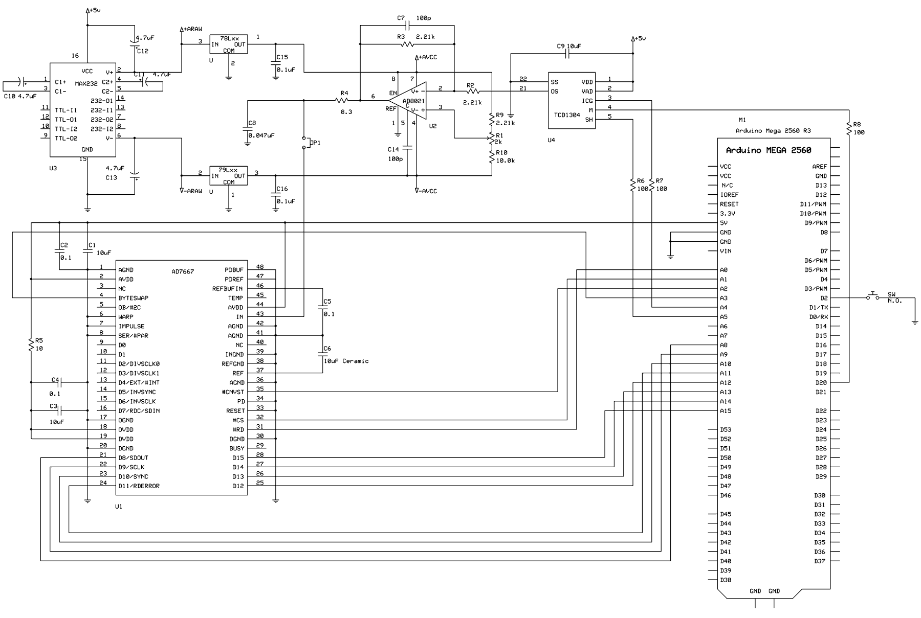
16 bit version
#include <util/delay_basic.h>
#define RD (1<<0)
#define CS (1<<1)
#define CNVST (1<<2)
#define BYTESWAP (1<<3)
#define ICG (1<<4)
#define SH (1<<5)
#define MCLK (1<<6)
// Full frame, including dark pixels
// and dead pixels.
#define PIXEL_COUNT 3800
#define CLOCKS PORTF
#define CLOCKS_DDR DDRF
#define DATA_PINS PINK
#define DATA_PORT PORTK
#define DATA_DDR DDRK
// 10mS exposure time.
#define EXPOSURE_TIME 1
// Initial clock state.
uint8_t clocks0 = (RD + CS + CNVST + ICG);
// 16-bit pixel buffer
uint16_t pixBuf[PIXEL_COUNT];
/*
* readLine() Reads all pixels into a buffer.
*/
void readLine()
{
// Get an 8-bit pointer to the 16-bit buffer.
uint8_t * buf = (uint8_t *)pixBuf;
int x;
cli();
CLOCKS |= (RD + CS + CNVST + ICG + BYTESWAP + SH);
OCR2A = 5;
TCNT2 = 0;
PORTB &= ~0x02;
for (x = 0; x < PIXEL_COUNT; ++x)
{
CLOCKS ^= SH;
CLOCKS &= ~CNVST;
CLOCKS |= CNVST;
_delay_loop_1(4);
__asm__("nop\n\t");
__asm__("nop\n\t");
__asm__("nop\n\t");
CLOCKS ^= SH;
CLOCKS &= ~(CS + RD);
*buf++ = DATA_PINS;
CLOCKS &= ~(BYTESWAP);
*buf++ = DATA_PINS;
CLOCKS |= (RD + CS + BYTESWAP);
}
sei();
}
/*
* startLine() Toggles the clocks to shift the line
* into the CCD shift register.
*/
void startLine()
{
// Set ICG low.
CLOCKS &= ~ICG;
_delay_loop_1(5);
// Set SH high.
CLOCKS |= SH;
_delay_loop_1(5); // 10uS.
// Set SH low.
CLOCKS &= ~SH;
_delay_loop_1(10);
// Set ICG high.
CLOCKS |= ICG;
}
/*
* sendLine() Send the line of pixels to the user.
*/
void sendLine()
{
int x;
for (x = 0; x < PIXEL_COUNT; ++x)
{
Serial.println(pixBuf[x]);
}
}
/*
* cleanLine() Performs voodoo on the data.
* Looks for shot noise and replaces it with
* the previous pixel data. You might want to
* skip this if doing serious science. The blip
* might be your data.
*/
void cleanLine()
{
int x, fixes = 0;
for (x = 1; x < PIXEL_COUNT; ++x)
{
if (pixBuf[x] > (int)(pixBuf[x - 1] * 1.1))
{
if (++fixes < 10)
pixBuf[x] = pixBuf[x - 1];
}
else if (pixBuf[x] < (int)(pixBuf[x - 1] * 0.9))
{
if (++fixes < 10)
pixBuf[x] = pixBuf[x - 1];
}
else
{
fixes = 0;
}
}
}
/*
* setup()
* Set the data port to input.
* Set the clock port to output.
* Start timer2 generating the Mclk signal
* Set the pullup on pin 2 for the start switch.
*/
void setup() {
CLOCKS_DDR = 0xff;
CLOCKS = clocks0;
DATA_DDR = 0x0;
Serial.begin(115200);
// Setup timer2 to generate a 1.333MHz frequency on D10
TCCR2A = (0 << COM2A1) | (1 << COM2A0) | (1 << WGM21) | (0 << WGM20);
TCCR2B = (0 << WGM22) | (1 << CS20);
// "5" causes 6 intervals - 0 through 5
OCR2A = 5;
TCNT2 = 0;
// Output Mclk on D2
DDRB |= 0x10;
// For the trigger switch.
pinMode(2, INPUT_PULLUP);
}
/*
* loop()
* Read the CCD continuously.
* Upload to user on switch press.
*/
void loop() {
startLine();
readLine();
delay(EXPOSURE_TIME);
if (!digitalRead(2))
{
cleanLine();
sendLine();
}
}
Discussions
Become a Hackaday.io Member
Create an account to leave a comment. Already have an account? Log In.