 Ulrich
Lets bring this schematic to a PCB Design.
I started doing PCB Designs in University. Back in the time I was using Eagle or Altium.
In the last couple of years the Open Source tools have become better and better.
Thats why I choosed KiCad for my hobby projects.
Once finished with the schematic you need to start a new PCB Design with the Tool PCBNEW
This opes a drawings program where you can add all you components.
No the fun part begins.Place all your components so that you can still solder them and you may route the signal lines.
At the end. Add a Ground plane and think about thermal and EMC.
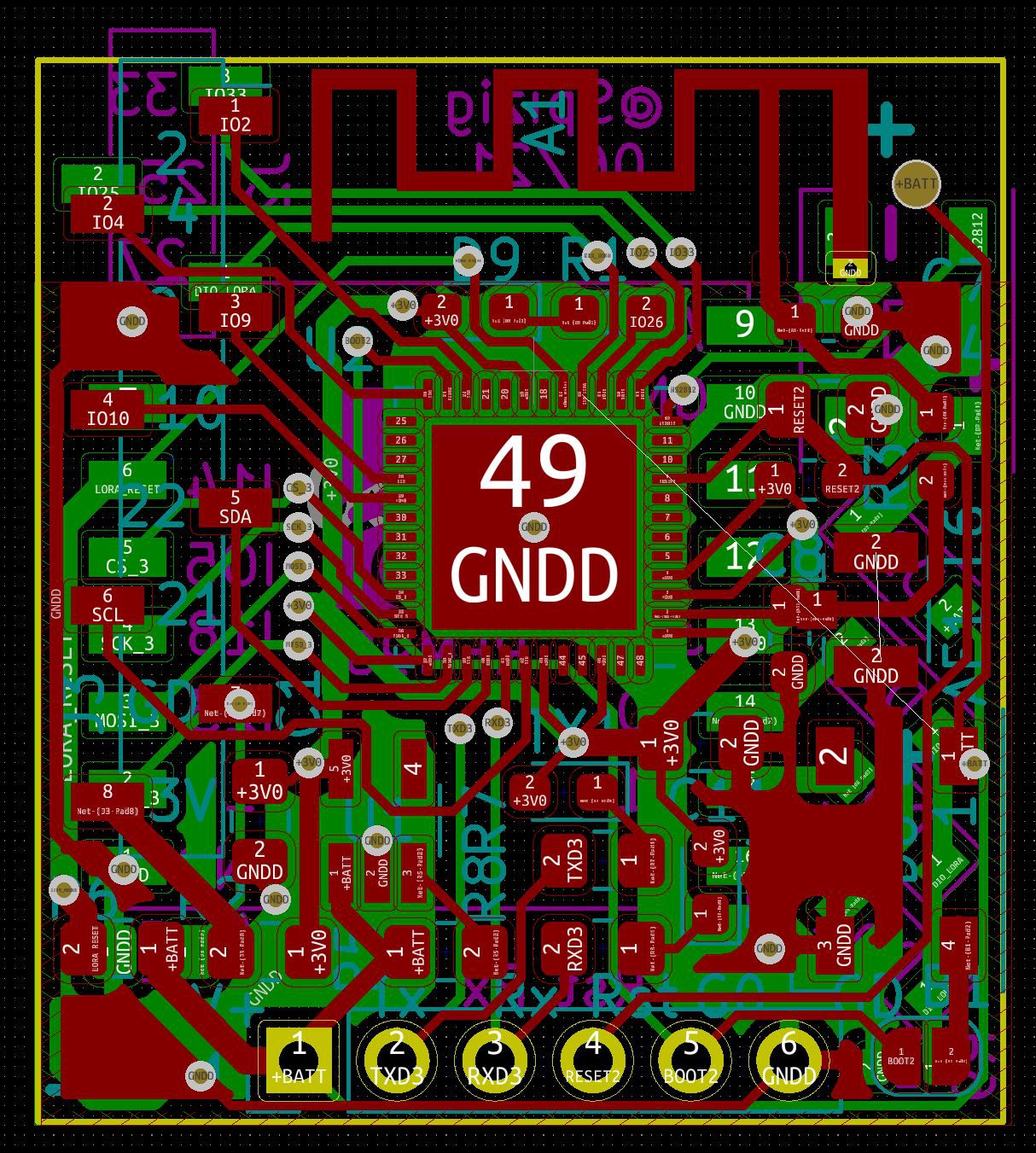
You may see that there is one line on the bottom side of the Board which is not routed. I did this on purpose. This line is not needed all the time and i can add this line later on with an Air wire if needed.
Discussions
Become a Hackaday.io Member
Create an account to leave a comment. Already have an account? Log In.