 agp.cooper
Hardware CHUMP
CHUMP stands for "Cheap Homebrew Understandable Minimal Processor".
It is the invention of Dave Feinberg and described in his paper "A Simple and Affordable TTL Processor for the Classroom".
I am not a fan of Control ROMs for simple computers. So this project looks at a hardware control version of CHUMP.
Original CHUMP Instruction Set
The original CHUMP had the following instructions:
| OpCode | Instruction | Comments |
| 0000 | LOAD const | ACC = CONST; PC++; |
| 0001 | LOAD mem | ACC = MEM[ADDR]; PC++; |
| 0010 | ADD const | ACC = ACC PLUS CONST; PC++; |
| 0011 | ADD mem | ACC = ACC PLUS MEM[ADDR]; PC++; |
| 0100 | SUBTRACT const | ACC = ACC PLUS CONST; PC++; |
| 0101 | SUBTRACT mem | ACC = ACC PLUS MEM[ADDR]; PC++; |
| 0110 | STORETO const | MEM[ADDR] = ACC; PC++; |
| 0111 | STORETO mem | MEM[MEM[ADDR]] = ACC; PC++; |
| 1000 | READ const | ADDR = CONST; PC++; |
| 1001 | READ mem | ADDR = MEM[ADDR]; PC++; |
| 1010 | GOTO const | PC=CONST; |
| 1011 | GOTO mem | PC=MEM[ADDR]; |
| 1100 | IFZERO const | IF (ACC==ZERO) THEN PC=CONST ELSE PC++; |
| 1101 | IFZERO mem | IF (ACC==ZERO) THEN PC=MEM[ADDR] ELSE PC++; |
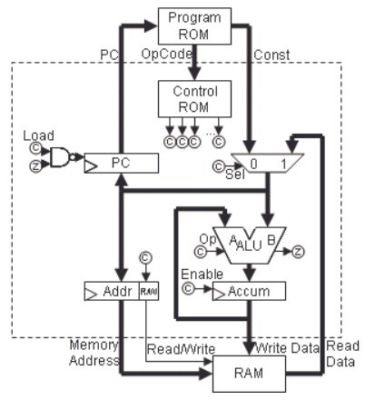
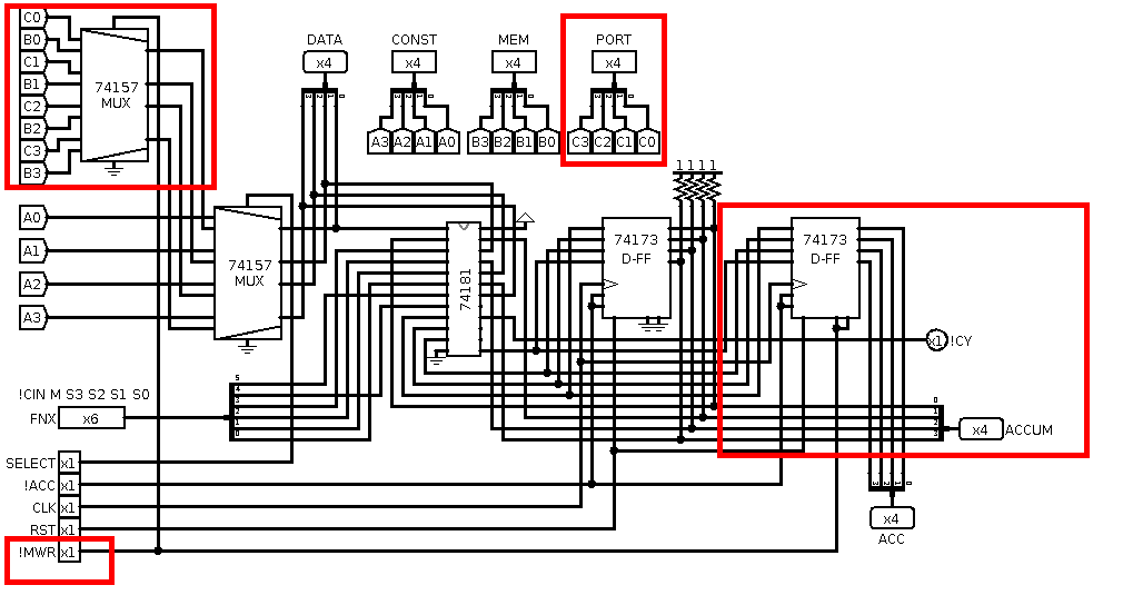
The Original CHUMP Data Flow Diagram
Here is the Original CHUMP data flow diagram:
Harvard Architecture
CHUMP uses the Harvard Architecture which means the program is in Read Only Memory (ROM) and data is in Random Access Memory (RAM). It is not possible for CHUMP to self program. All programs must be written to an Erasable Programmable ROM (EPROM).
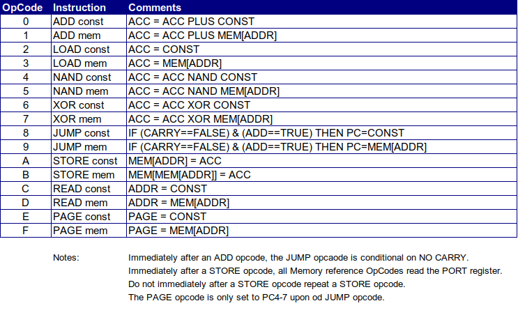
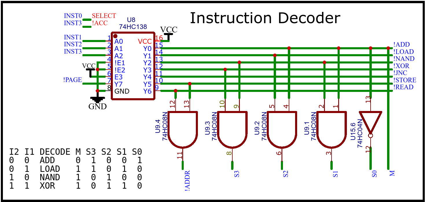
Extended Instruction Set
To reduce the hardware logic complexity I have reworked the instruction set:
| OpCode | Instruction | Comments |
| 0000 | ADD const | ACC = ACC PLUS CONST |
| 0001 | ADD mem | ACC = ACC PLUS MEM[ADDR] |
| 0010 | LOAD const | ACC = CONST |
| 0011 | LOAD mem | ACC = MEM[ADDR] |
| 0100 | NAND const | ACC = ACC NAND CONST |
| 0101 | NAND mem | ACC = ACC NAND MEM[ADDR] |
| 0110 | XOR const | ACC = ACC XOR CONST |
| 0111 | XOR mem | ACC = ACC XOR MEM[ADDR] |
| 1000 | JNC const | IF (!CARRY=HIGH) THEN PC=CONST |
| 1001 | JNC mem | IF (!CARRY=HIGH) THEN PC=MEM[ADDR] |
| 1010 | STORE const | MEM[ADDR] = ACC |
| 1011 | STORE mem | MEM[MEM[ADDR]] = ACC |
| 1100 | READ const | ADDR = CONST |
| 1101 | READ mem | ADDR = MEM[ADDR] |
| 1110 | PAGE const | PAGE = CONST |
| 1111 | PAGE mem | PAGE = MEM[ADDR] |
I have replaced SUBTRACT with NAND. NAND is necessary for bit operations such as AND and OR etc. I have added XOR as it takes too many instructions to generate it from NAND instructions.
Subtraction can be modeled as:
SUB ? = NAND -1; ADD ?; NAND -1
I have added a PAGE instruction to extend the ROM capacity to 256 bytes. The PAGE register is preloaded but only sets the upper 4 bits of the program counter upon a jump.
I have replaced GOTO and IFZERO with JNC (Jump on Not Carry). The not carry and jump logic only works immediately following an ADD instruction. Otherwise the JNC is unconditional (i.e. always jumps).
The carry flag is necessary for double precision arithmetic and can replace the zero flag for loops and comparison operations with code modification.
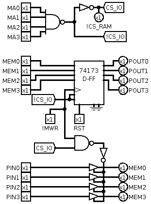
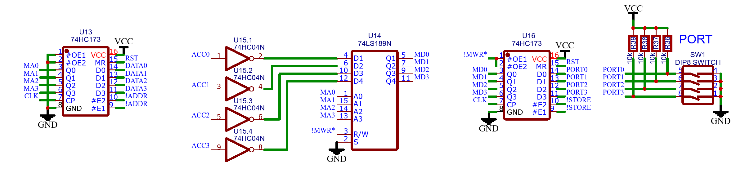
Port Input and Output
There is no Input and Output (I/O) command at the moment. It is proposed to map I/O space over RAM space (say address 0x0F).
Upon review, I find I can use any memory reference instruction immediately after a STORE instruction to read an input port.
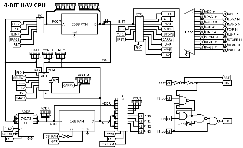
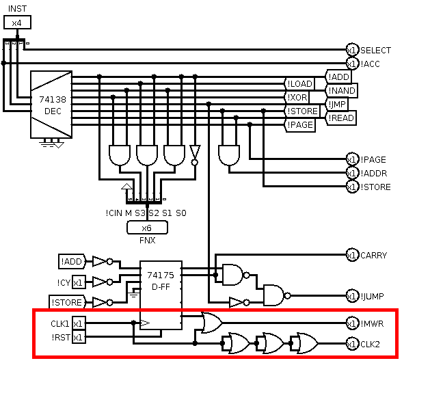
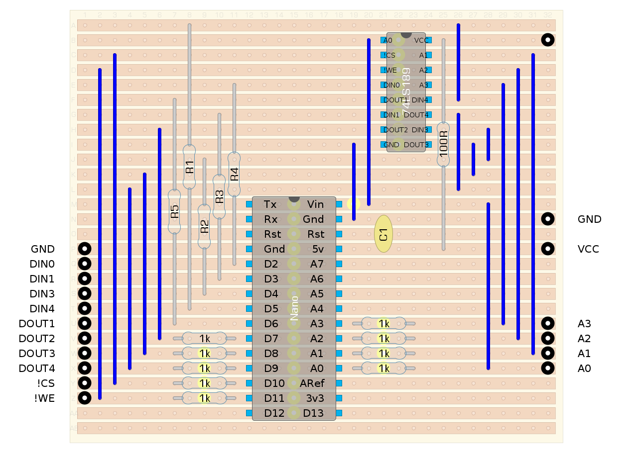
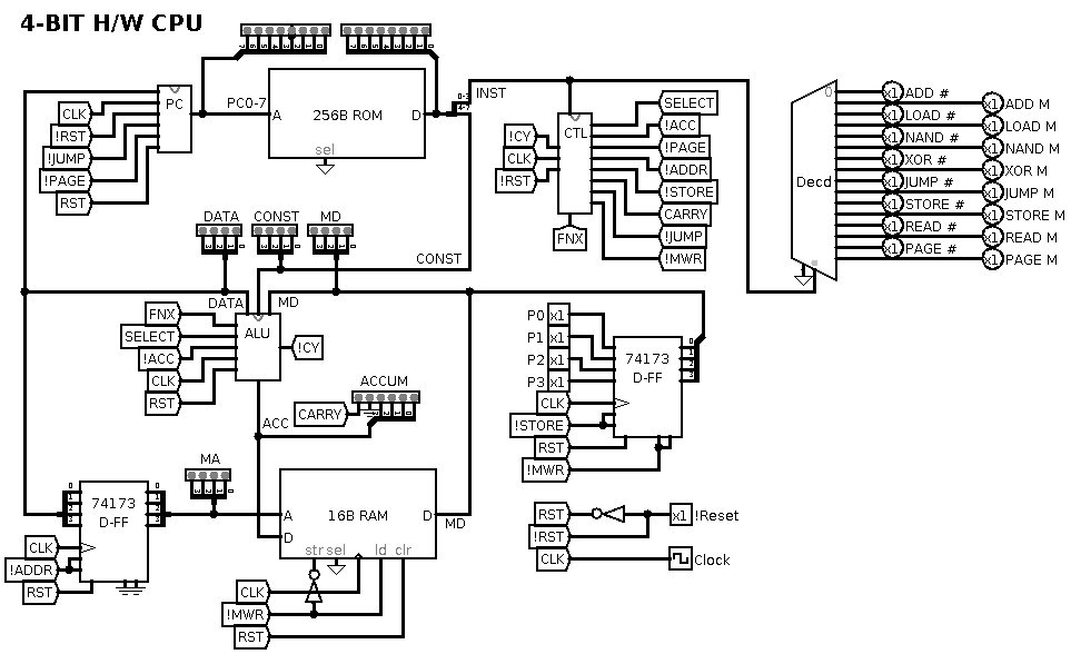
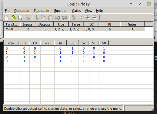
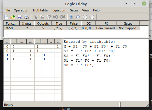
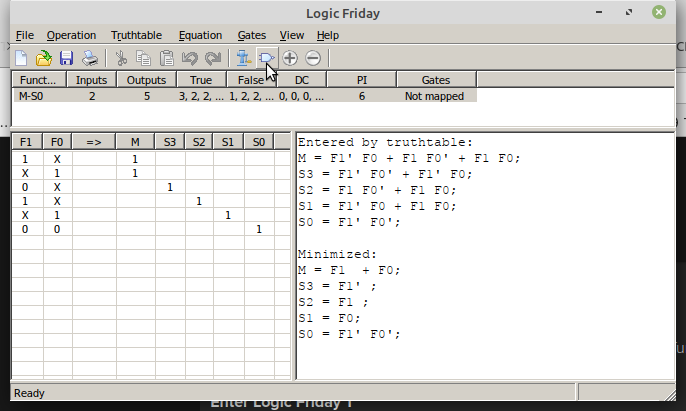
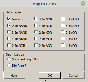
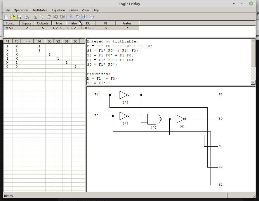
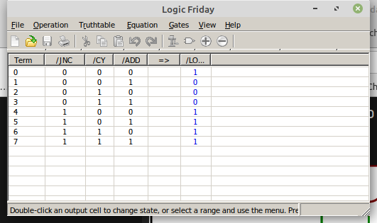
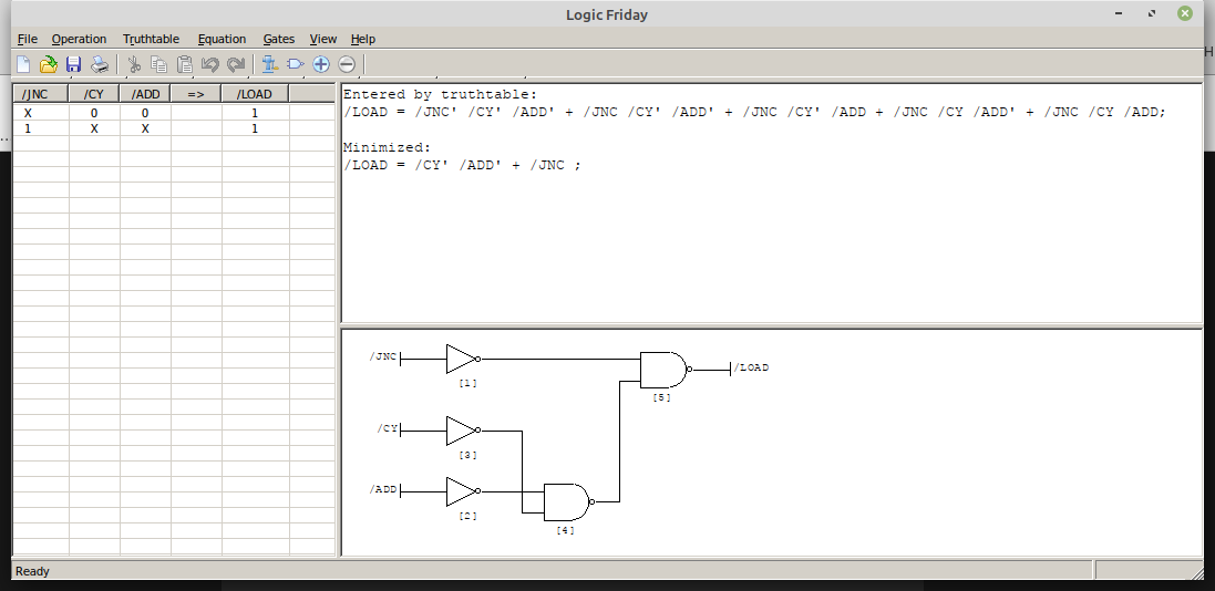
Control Logic
Here is my version of the control logic:
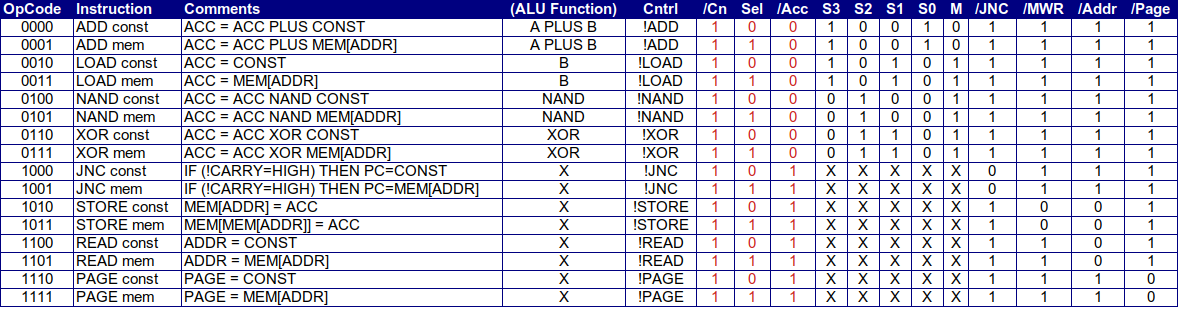
For the Hardware Control Logic, the following schematic was developed:

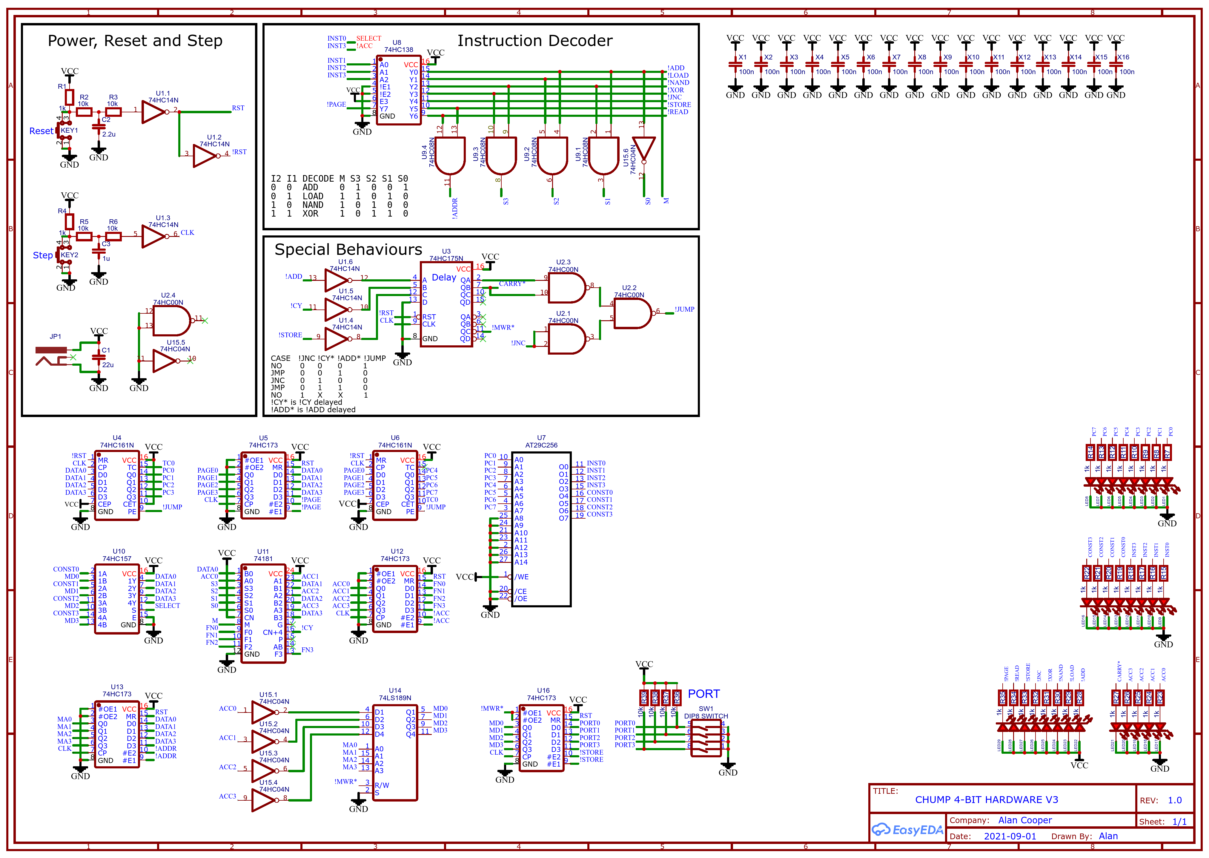
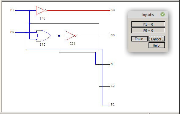
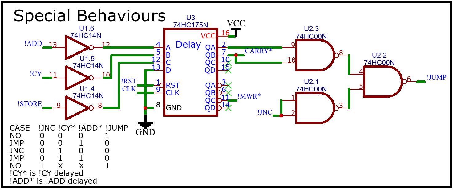
Special Behaviours
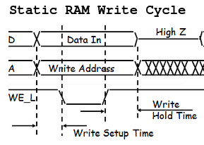
To get the required (special behaviours) logic for the JNC/ADD (!JUMP) and RAM write signal (!MWR), the follow logic was used:

The main problem was latching or delaying the action until the next clock cyle.
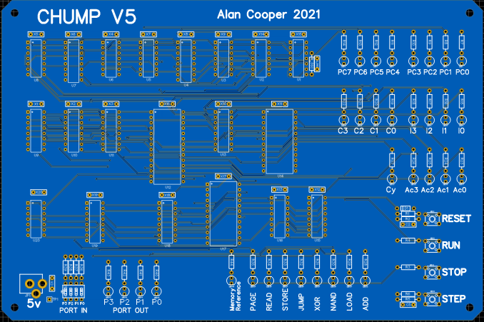
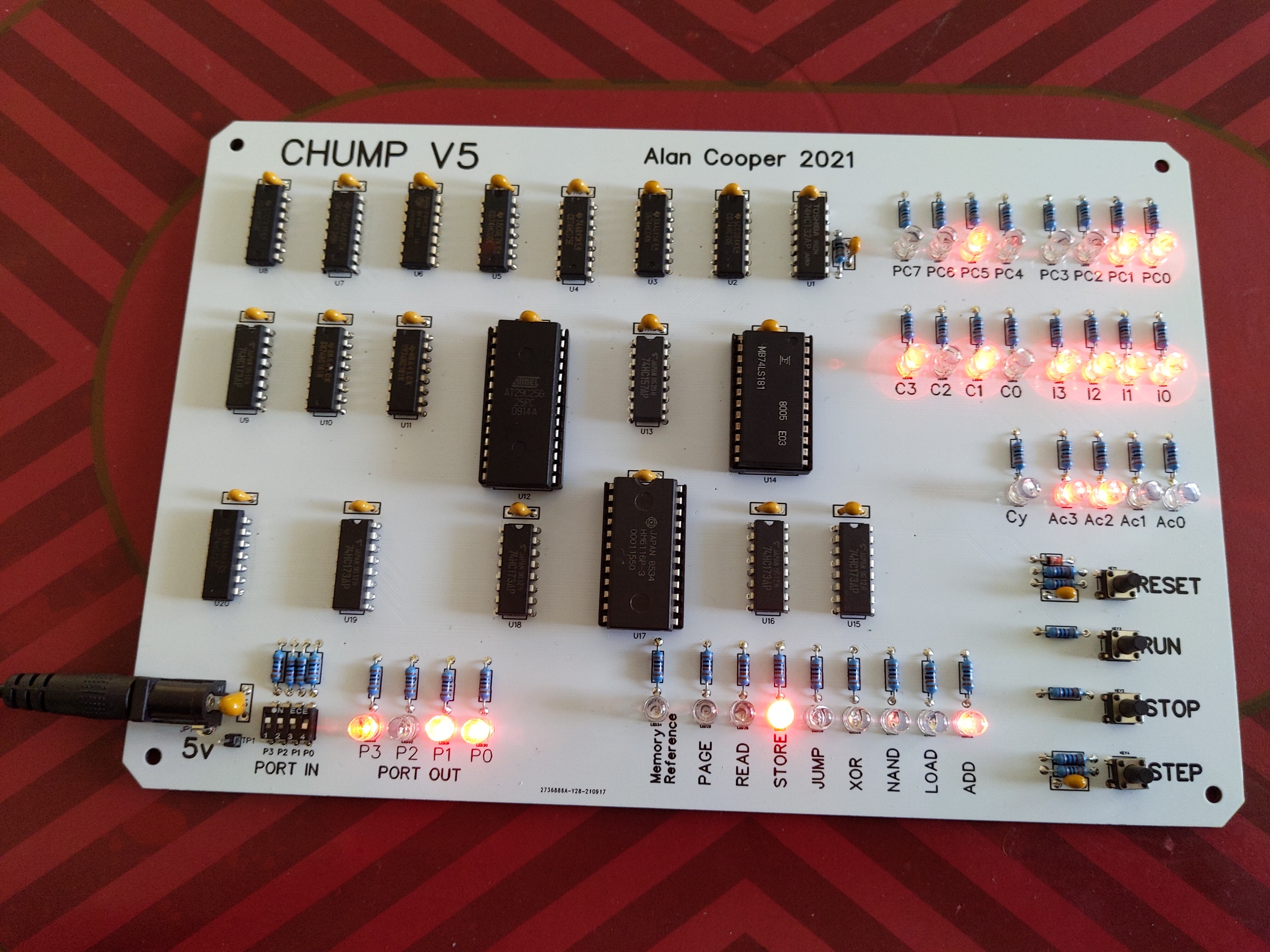
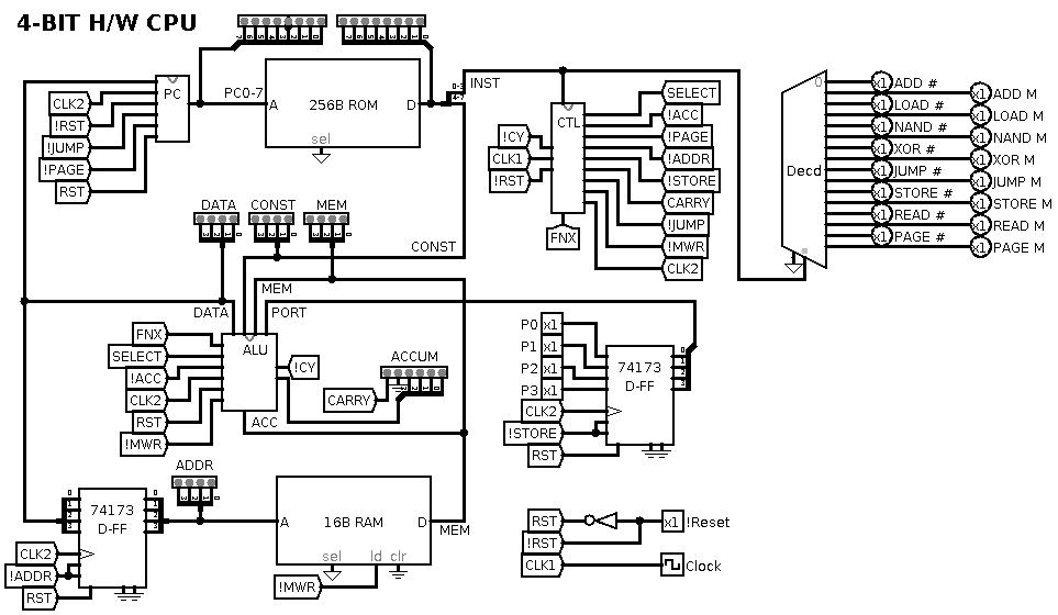
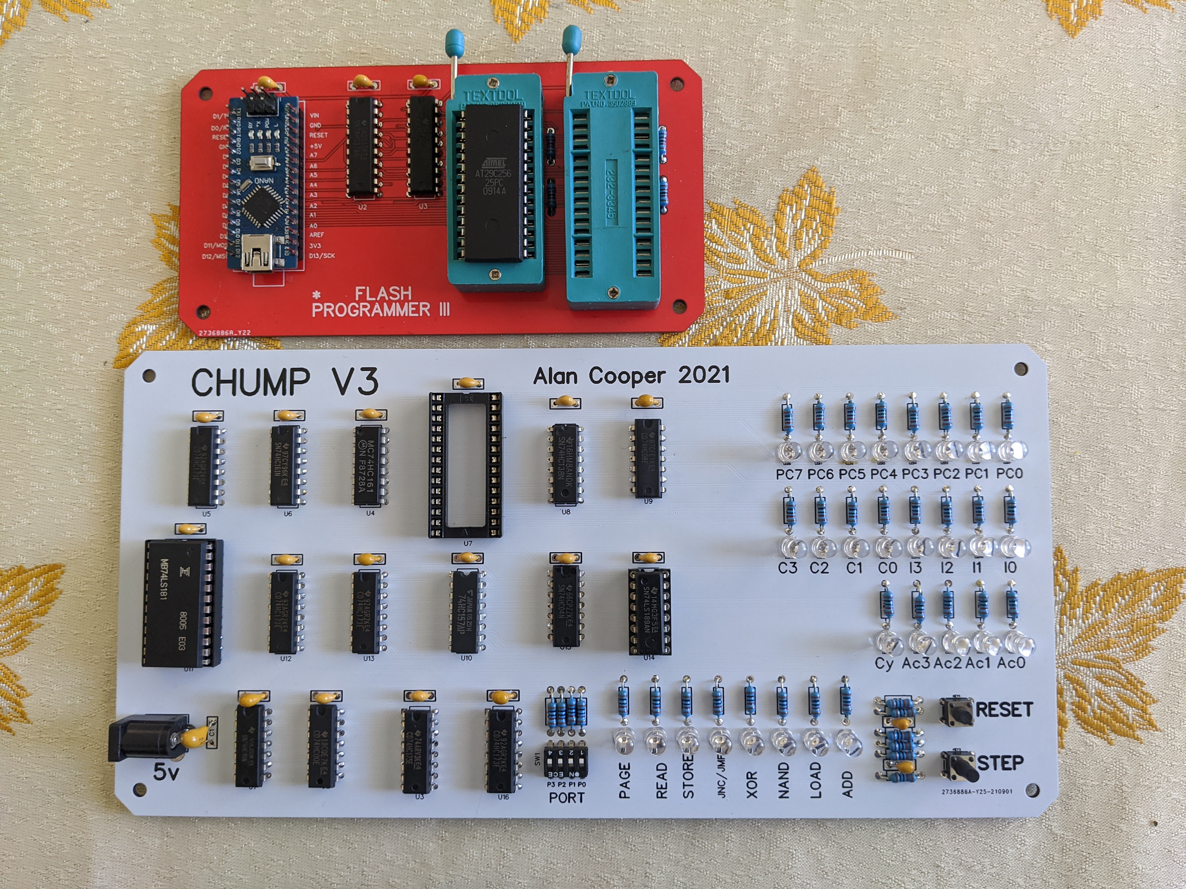
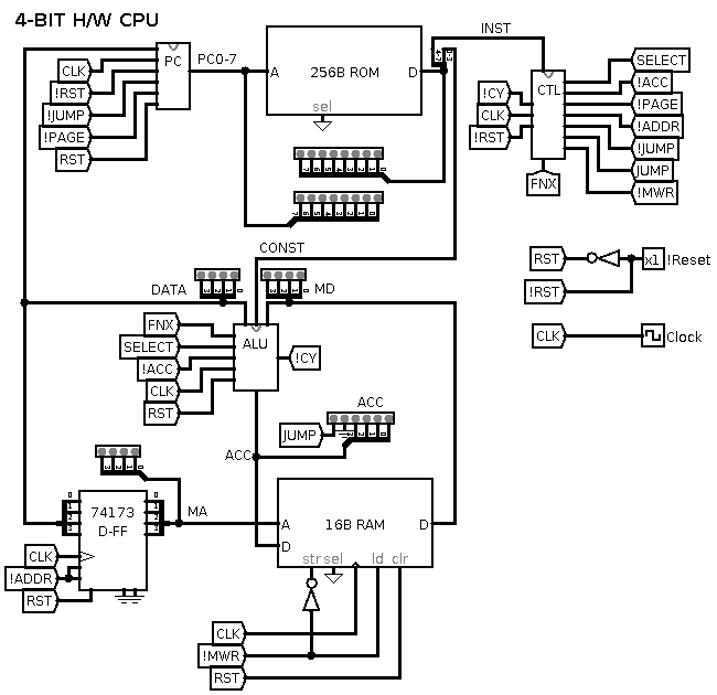
CHUMP V3 Hardware Schematic
Here is the schematic:
Final Comments
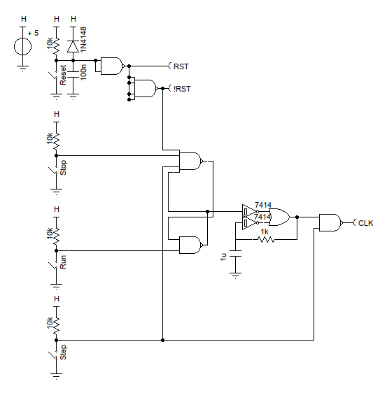
Final comments before implementation.
The clock is manual, each press cycle...
Read more »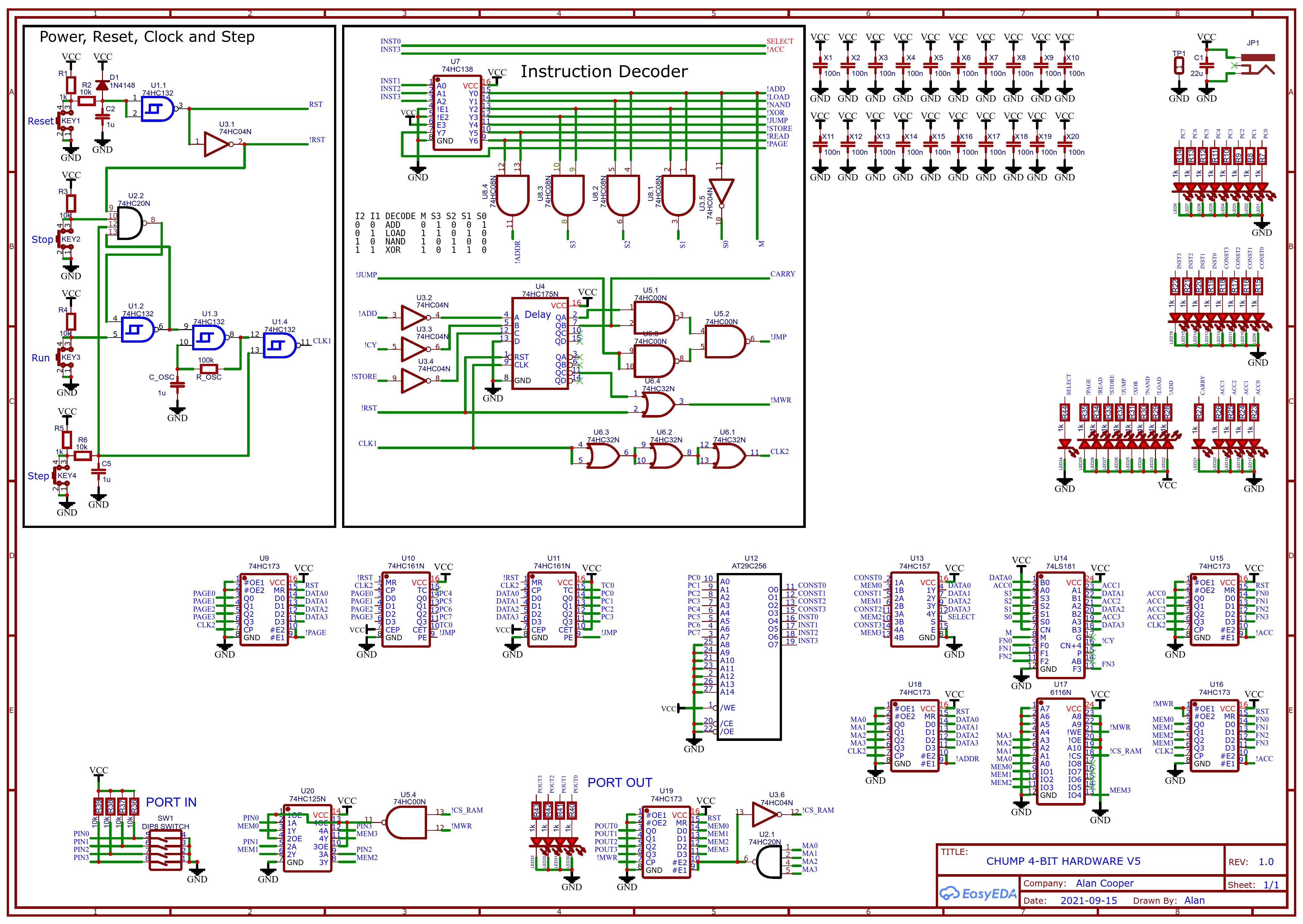


 zaphod
 spudfishScott
 Michael Möller