 agp.cooper
The Static RAM Write Cycle Timing
For static RAM, usually the write pulse starts after the address changes and write pulse finishes before the address changes to the next address:
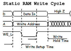
The original CHUMP design uses a 74LS174 (Hex D-Latch) to clock each cycle, the memory address AND the memory read/write control. This works because most memory chips have a near zero "Write Setup Time" and near zero "Write Hold Time", AND the all the signals change at exactly the same time (as they are clocked by the same 74LS174 d-latch).
For my design I have separated the address d-latch and the read/write control d-latch. Therefore I have to ensure that both chips clock at the same time.
One problem is a slowly rising clock can cause the separate d-latchs not to clock at the same time. This has been eliminated by the use of the 74HC14 schmitt-trigger for the clock and reset circuity.
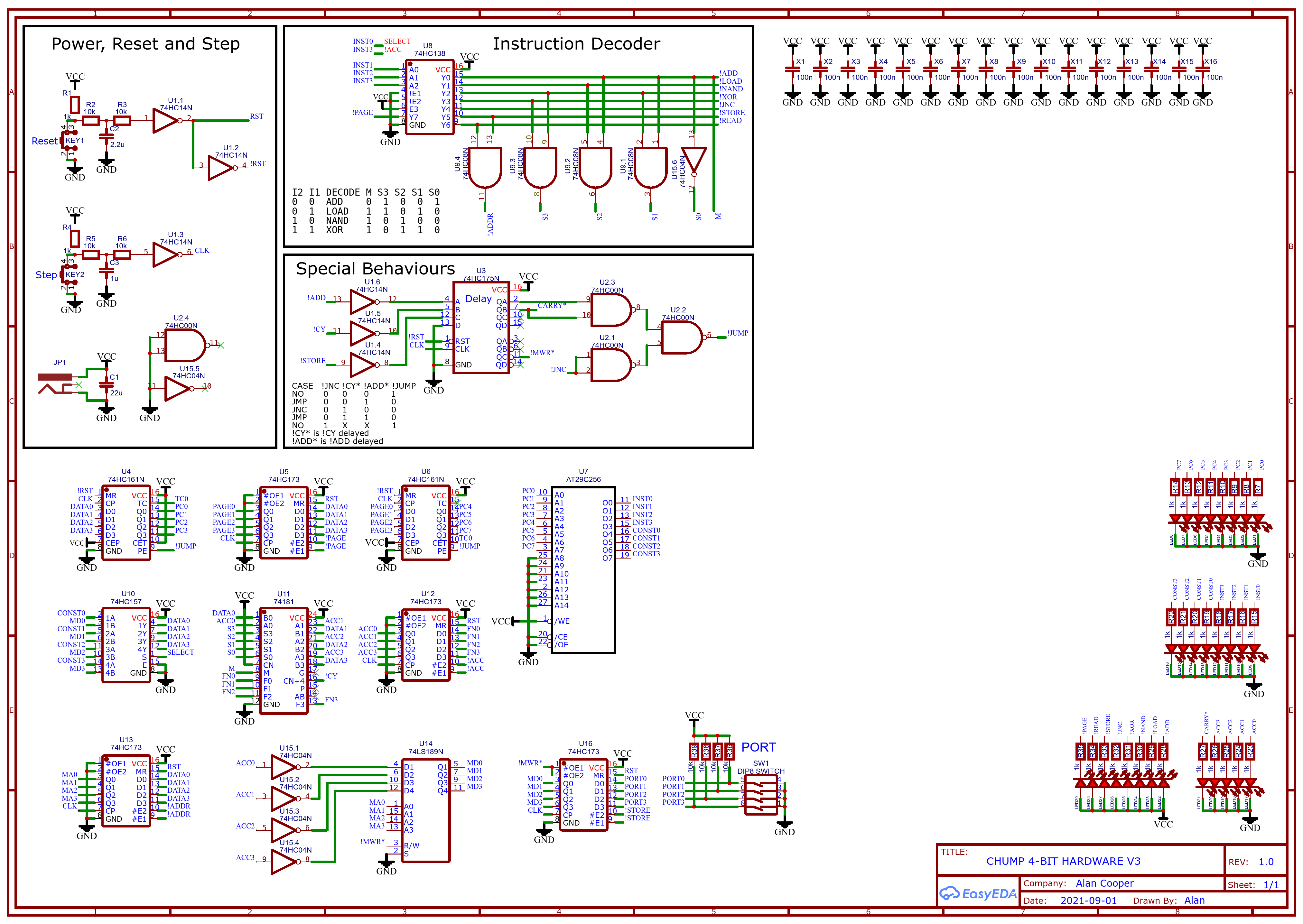
Another problem is a different propagation delay for the memory address and the read/write control. This has been minimised as both paths have the same (nominal) propagation delay (17ns), refer to U3 and U13, going to U14 in the revised schematic (around U3):
Finally, logic chips can tolerate small glitches if they are less than the propagation delay (say <8ns). This is based on the minimum clock pulse width of 7ns to 8ns for 74HC logic family.
An additional protection is that the 74LS189 memory chip has a typical 25ns minimum write pulse width.
AlanX
Discussions
Become a Hackaday.io Member
Create an account to leave a comment. Already have an account? Log In.
Hi Ken,
I would say all memory devices latch on the trailing edge.
The issue is that changing the address while the write is active is illegal and can result in an unpredictable writes.
The CPU issue is that the instruction cycle is only one clock cycle.
I did an earlier version that had the clock generate a write pulse as well as a clock pulse.
But really the purpose of the blog was to highlight that it can work with precautions.
Regards Alan
Are you sure? yes | no
One begins to understand why some CPUs have phases in the instruction cycle.
Are you sure? yes | no
What about using a level sensitive latch instead of an edge triggered latch for the write logic? Then the data has only to be valid at the trailing edge.
Are you sure? yes | no