 Colin Maykish
I've been mostly happy with the hardware design of Herring, but I want to make some minor changes:
1. The reset button must be pressed after power on for the system to reliably initialize. This is not a great experience. It would be better if the system could reset fully when power is applied.
2. There are a few small fixes I want to make on the backplane. The first is to remove the regulator and replace it with a direct 5v power connection. USB would be ideal. Even better would be to have an on-board USB-to-serial chip, allowing a single USB connection for serial and communications.
3. Replace some single-chip boards with combination boards to save backplane slots.
My secondary goal is to preserve the system header pinout as much as possible to maintain at least some backward compatibility with the existing PCBs.
Here are the new PCB designs I'm working on. First is the new backplane:
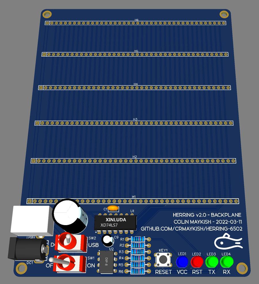
As mentioned, the biggest difference here is the addition of a 555 power-reset circuit and a MCP2221A USB-to-serial chip. The added USB-B socket can now provide power and serial to the host PC with a single cable. Since the actual UART chip will still be on a daughterboard, I've had to sacrifice two of the decoder pins on the system bus for the TX and RX lines that feed this converter. Finally, there's a DC adapter for regulated 5v input just to leave the option open. The second switch selects between power from USB or the DC input.
Next up is what I'm calling the core system board. It's a mashup of the old CPU board and the two slot memory boards.
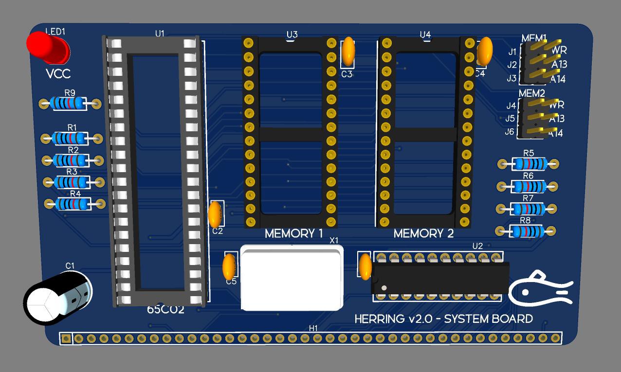
Not much to say about this one. It's the CPU, two memory ICs with selectable size and write-enable, and the oscillator and GAL. The GAL is responsible for selecting the on-board memory, but it also connects to the decoder lines on the system bus.
Finally, the new "I/O" board:
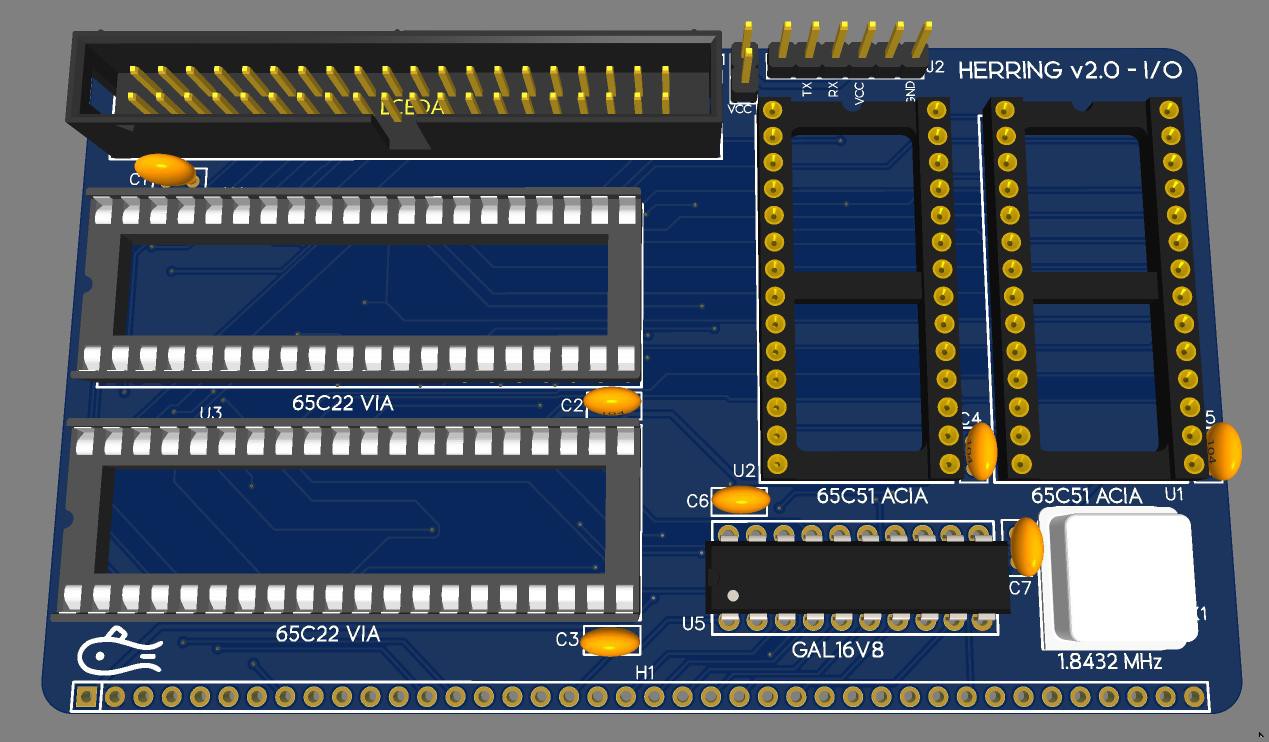
Again, this is just a combination of two VIAs and two ACIAs with an additional GAL. This GPIO lines from both VIAs are connected to the 40-pin ribbon cable header. One of the ACIAs has a breakout header and the other is connected to the system bus directly to feed the USB-to-serial adapter on the backplane. This single board is equivalent to four boards of the previous design.
I'm still working on some accessory boards to go along with these and the designs need to be double checked, but I'm planning to order the first batch this week.
Discussions
Become a Hackaday.io Member
Create an account to leave a comment. Already have an account? Log In.