 Mitsuru Yamada
1. Circuit of the SAR ADC
Figure 1 shows the SAR ADC board and Fig. 2 is the schematic.
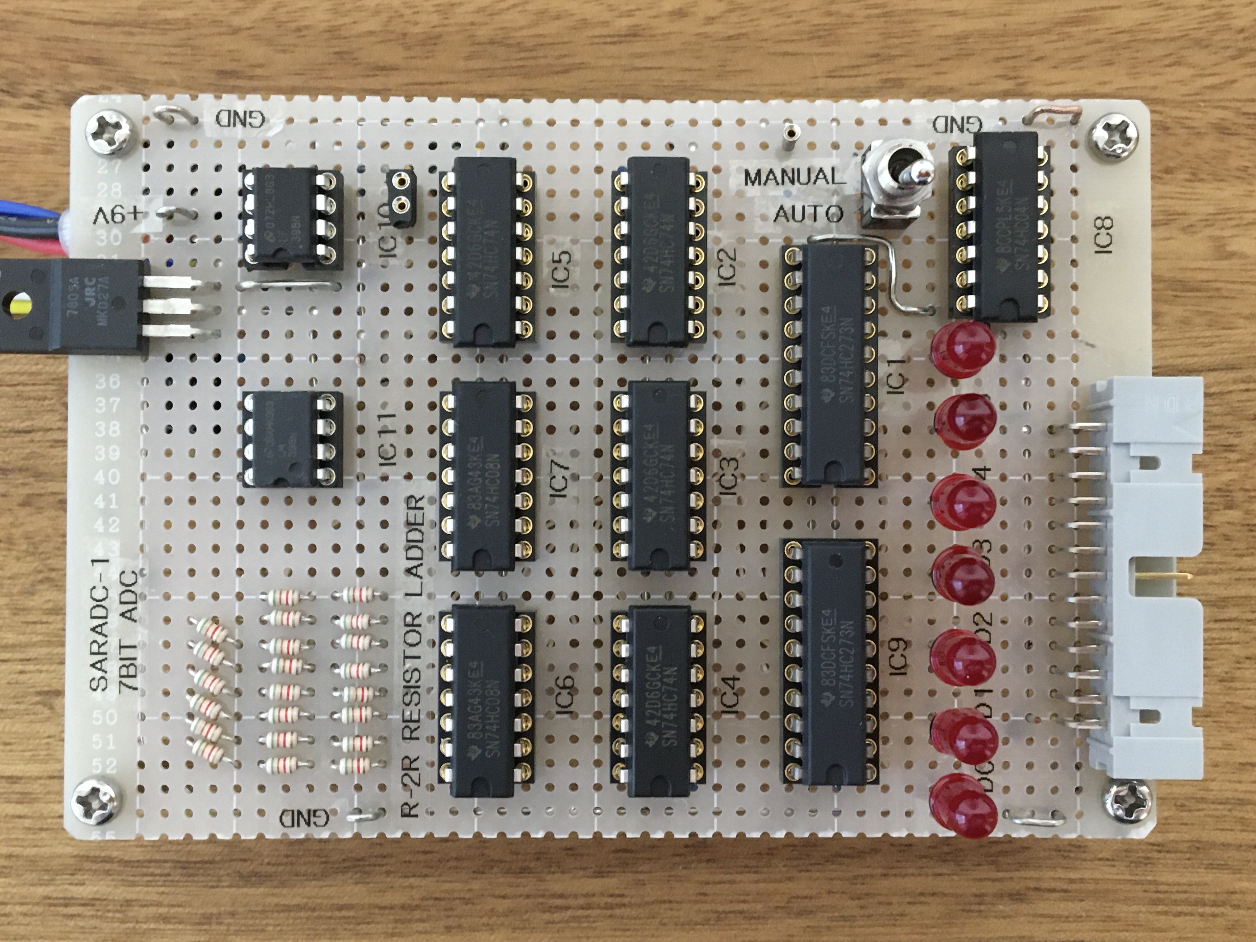
Fig. 1 Circuit board of the SAR ADC
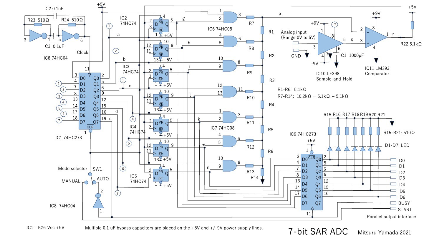
Fig. 2 Schematic of the SAR ADC
The IC1 is an 8-bit shift register. The IC2, 3, 4, and 5 are D-FFs to hold the comparison result of the comparator IC11. The IC6 and IC7 are gates that take the logical product of the shift register output and the D-FF output. The IC9 is a register for holding the AD conversion result. The D1 to D7 are LEDs for displaying the binary data of conversion results. The clock to operate the SAR is generated by an astable multivibrator configured with IC8. The clock period is 103 us and the conversion time is 824 us. The dynamic range of the input signal is from 0 V to 5 V and the output bit width is 7-bit. 0 V is converted to binary '0000000' and 5 V to '1111111'.
2. Internal DAC
The internal Digital to Analog Converter (DAC) that generates the comparison signal with the input signal was configured with R-2R resistor ladder. Normally, it is preferable to use fixed register ladder networks, which have high accuracy, but here, for training purposes, I used individual resistors. The dispersion of the resistors is 1% in actual measurement.
3. Sample-and-Hold
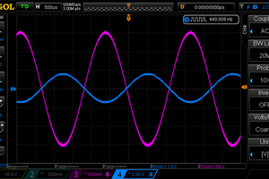
If the input signal changes during conversion, the conversion result will be incorrect, so the ADC needs a sample-and-hold. The sample-and-hold can be composed of an op amp and a FET switch, but here I used a monolithic IC, LF398 [2]. Fig. 3 shows an example of a sine waveform input signal and sample-and-hold output signal displayed on an oscilloscope.
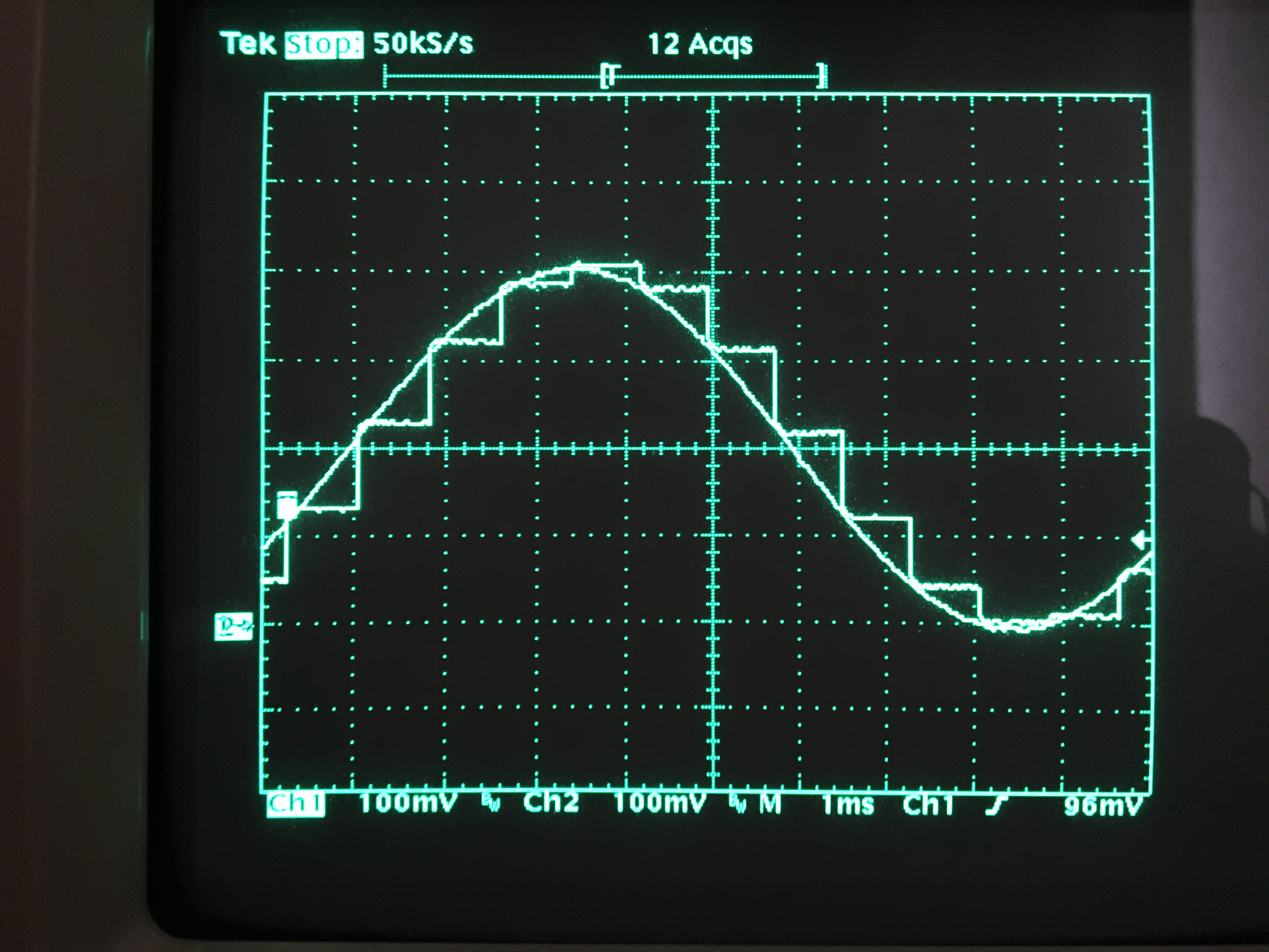
Fig. 3 Sine input signal and sample-and-hold signal.
4. Operation of the SAR
Figure 4 shows the SAR timing. The lowercase symbols in the figure correspond to the symbols of the signals in the schematic in Fig. 2.
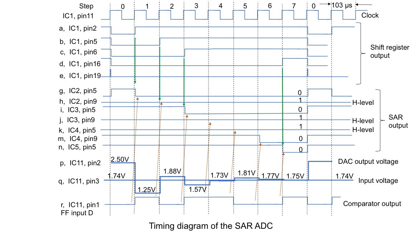
Fig.4 Timing diagram of the SAR ADC
As shown in ‘a’ to ‘d’ of Fig. 4, the shift register of IC1 supplies the rising edge signals, which is shifted by one clock, to the trigger input of D-FFs. This trigger signal causes the D-FF to hold the judgment result of the comparator, as shown in ‘g ‘to ‘n’ in Fig. 4.
In the first step 0 of the SAR operation, all the output bits of the shift register IC1 are cleared to zero, and the output bits of the D-FFs of IC2 to IC5 are all preset to '1'. Each time it move to the next step, the next bit of the shift register is set to ‘1’, and the output of the DAC is add or subtract with a weighting by half of previous, and a judgment is made as to whether it is large or small in relation to the input signal.
The following example shows a case where the input signal is 1.74V. At the beginning of the conversion operation of the step 0, a 2.5V signal, which is half of the dynamic range ('1000000'), is output from the DAC and compared with the input signal by the comparator. Since the comparison signal is larger than the input signal in the step 0, the comparator output 'r' becomes '0'. Then the D-FF output 'g' becomes '0' in the next step 1.
This results...
Read more »


 RoGeorge
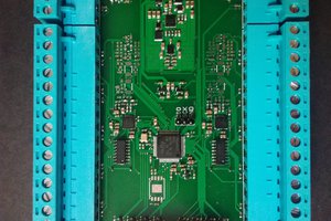
 NotBlackMagic
 Yann Guidon / YGDES
 doctek
Cool project!