 Dan Maloney
 OK, everyone, let's get started. I'm Dan and I'll be the moderator today along with Dusan for Mark Hughes and Greg Ziraldo. They're both from Advanced Assembly and they're here today to talk about big copper. Welcome!
 Hi everyone! I'm Mark
![]() Hi, Mark...
Hi, Mark...
I work with Greg at Advanced Assembly in beautiful Auroroa, Colorado. We are the original quick-turn industry experts, and we make boards as fast as you need them -- including in a single shift.
So maybe we can start with a little about your backgrounds?
I type too slow ;-)
We're so big, we have our own pick teams at the major parts distributors -- so your parts are likely going to show up the same morning that your parts are.
We can stuff 'em and get 'em back on the plane back out to you.
We're here to answer anything you want to know about Heavy Copper (generally regarded as 1.5 oz or greater)
And we can help you solve any other PCB and PCBA problems you might have.
 Glad to be here Dan! Hi everyone, I'm Greg. I am over Operations (engineering, manufacturing and supply chain) at Advanced Assembly. I have been with AA for a little over 4 years and I have been in the high-reliability side of EMS for nearly 18 years.
So the line between heavy and regular copper is pretty slim, right? Aren't most boards 1-oz?
I've got this Greg.
Most boards are 0.5 oz to 1 oz and are plated with an additional 0.5-0.7-1.0 oz of copper (to make the vias).
 My main question is, that ludicrous board with 3D soldermask: is most of that copper weight plated (I think it was 12oz)?
I'm looking for a better graphic to illustrate the point.
The board in the picture I used was a 20-oz board, IIRC
That is too many ounces.
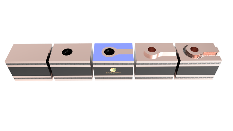
But all boards start out as copper sheets, we put a photo-imagable mask on it, and project a negative image of your artwork with fancy scanning lasers. That makes the mask tough and impenetrable.
Just an impossible number of ounces.
https://hackaday.com/2016/12/16/massive-20-oz-copper-pcb-enables-electric-racing/
Massive 20-oz. Copper PCB Enables Electric Racing
Is twenty times the copper twenty times as much fun to work with? Ask [limpkin] and follow along as he fabricates a DC/DC block for a Formula E race car on 20-oz copper PCBs. The typical boards you order from OSH Park and the like usually come with 1-ounce copper - that's one ounce of copper cladding per square foot of board.
Then it goes in electroplating tanks where we build up the traces and vias.
I my experience that would have to plated up. I have never seen a board with that high of Cu weight!
What's the heaviest y
y'all do?
Finally, we put the whole thing in a tank of acid and etch away copper from everywhere. The parts we plated survive the etch.
Plating takes time.
4-6oz is the safe area
We have 4 oz sitting on the shelf right now, usually, but not always have 6oz on hand too. Then that can be plated up.
But.
4 oz can be bought of the shelf without plating.
There's a lot of reasons you shouldn't.
How long would that take? Seems like electroplating is a slow process. I'd think slow is the last thing you want in a quick-turn environment.
I mean, the biggest reason is that Greg will make fun of you. And you dont' want that.
![]() I imagine minimum trace clearances and traces widths increase with copper weight. What are general rule of thumbs for say 4 oz and 6 oz?
I imagine minimum trace clearances and traces widths increase with copper weight. What are general rule of thumbs for say 4 oz and 6 oz?
We've got some cool pulse-plating tech. But it'll add a couple days to your turn time.
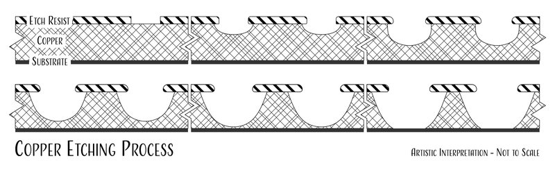
 Assuming with very thick copper on pcbs, that it's still etched, does the etchant not try to eat into the sides of the traces, because they're so tall vertically? (hope that makes sense)
DC plating can take ~2+ hours per basket. Pulse plating cuts that in half and better plating control.
To the designers out there, what applications are you using heavy copper in your stack up for?
@anfractuosity yes!
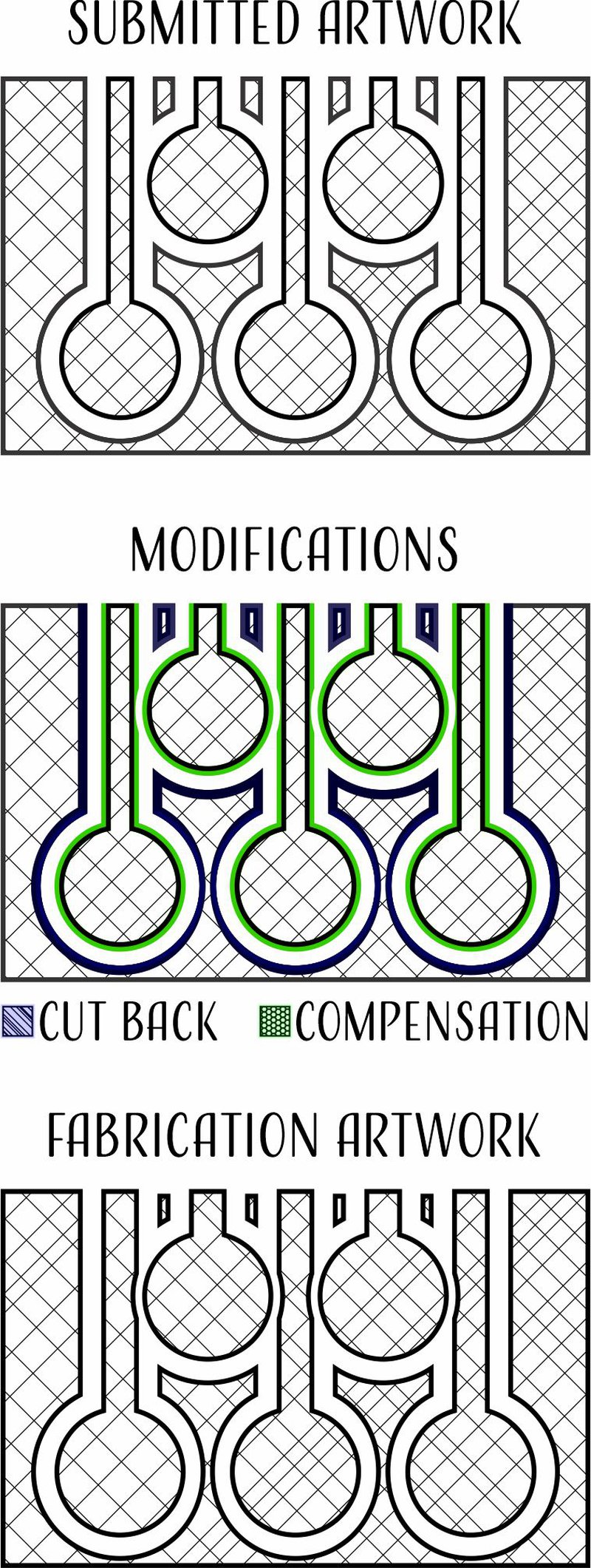
So there is etch compensation performed on all your artwork.
The dreaded undercutting
Yes ^^^
That will roll the trace right off of the laminate.
interesting cheers, 'etch compensation' means you make the traces appear a bit larger than necessary?
Yeah -- let me find you a pic to clear it up.
![]() @Greg Ziraldo : how do you handle vias for high current?
@Greg Ziraldo : how do you handle vias for high current?
What do you mean @echogee?
Greg's is a Grade-A fabricator. You call 'em out, he'll make 'em.
A robust via design starts with drill size, aspect ratio of the hole to the material thickness and via fill if VIP is part of your design.
![]() Traditional vias are 0.5oz thick right? So if current is supposed to transfer between layers, you'd need thicker vias ?
Traditional vias are 0.5oz thick right? So if current is supposed to transfer between layers, you'd need thicker vias ?
@echogee is this high-frequency current?
![]() nope. just HIGH current
nope. just HIGH current
Class 3 is 0.001" of copper in the barrel.
Almost seems like there would be through-hole copper rivets for such an application.
You're better off using multiple vias to reduce inductance. If it's high frequency AC, then the current travels along the outer barrel walls. You can fill the vias with cat crap for all the good it'll do you.
As for temperature of the via -- it'll closely match the trace temperature above and below the via.
The Via doesn't heat up hotter than the trace.
Source (https://amzn.to/3qvZ7mV)
Crap...referrer link again.
Let me fix that.
True. Your dielectric thickness is going to really come in to play here as well. High current must have appropriate layer to layer insulation
PCB Design Guide to Via and Trace Currents and Temperatures
PCB Design Guide to Via and Trace Currents and Temperatures [Douglas Brooks, Johannes Adam] on Amazon.com. *FREE* shipping on qualifying offers. PCB Design Guide to Via and Trace Currents and Temperatures
That actually brings up a question someone posted on the announcement page:
Don’t forget the effect of skin depth: Past a few hundred kHz, adding thickness to a trace doesn’t buy you any more conductivity. You need to add width (or Litz techniques) to get more conductivity.
Not a question so much as an observation, I suppose
Litz is a wire-weaving technique. I don't know how you'd apply that to individual traces.
But at high frequencies, you also need smooth copper, and the surface roughness becomes a factor.
Have we missed any questions along the way?
![]() @Greg Ziraldo : So thicker copper pcbs mostly use 0.5oz vias and multiple of them?
@Greg Ziraldo : So thicker copper pcbs mostly use 0.5oz vias and multiple of them?
![]() Seems like resistance of typical 0.2mm via is 1-2 mOhm
Seems like resistance of typical 0.2mm via is 1-2 mOhm
Not sure how to answer that one. @Mark J Hughes ?
Sure -- but he keeps pinging you.
:)
![]() In the example, PCB for the Formula E DC/DC it seems like there is lots of extra space to widen several traces vs building them higher. Would you suggest a lower weight and wider trace in that case?
In the example, PCB for the Formula E DC/DC it seems like there is lots of extra space to widen several traces vs building them higher. Would you suggest a lower weight and wider trace in that case?
Yes -- you're better off using multiple vias than one giant one.
@Jason The example was something Greg and I laughed at. It's ridiculous.
Yes -- there is a trade off between copper width and height.
But it's not linear.
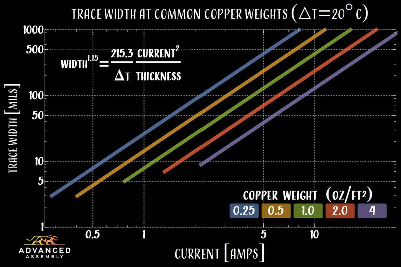
IPC-2221 used to be the designers bible for how to design trace thickness for a given weight of copper.
![]() On this page https://hackaday.com/2016/12/16/massive-20-oz-copper-pcb-enables-electric-racing/ the board price is $2250. How much of that is the large size (it looks large anyway) and how much is the extra plating? Is there some rule of thumb for adding X oz of copper per square inch of board (even if all of that square inch is not traces of course)?
On this page https://hackaday.com/2016/12/16/massive-20-oz-copper-pcb-enables-electric-racing/ the board price is $2250. How much of that is the large size (it looks large anyway) and how much is the extra plating? Is there some rule of thumb for adding X oz of copper per square inch of board (even if all of that square inch is not traces of course)?
The trouble is that it was based on some data collected by two underfunded scientists in the 50's/60's who made some of the data up because they didn't have money to run the experiments.
The whole "inner traces need to be twice as wide as outer traces" -- complete rubbish.
So about a decade ago, IPC-2152 committe did some experiments and generated new empiracle data
(BTW -- most online calculators still reference IPC-2221, don't use them)
@bboyes the material cost of the copper is insignificant compared to the manufacturing processes and labor to complete that.
They found a relationship between trace temp rise, copper weight and trace width.
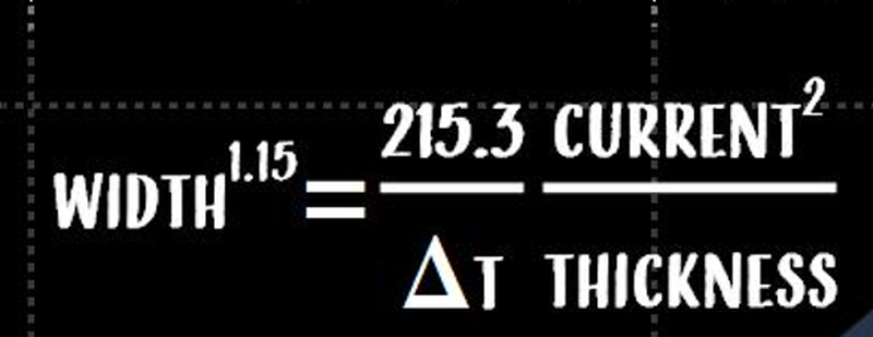
Greg and I rearranged the equations using two techniques.
1) I used math.
2) Greg used pure force of will.
![]() Got it. Is selective heavy copper an option worth considering or would it be better to stick with one weight? Would there be a likely quantity crossover where it is viable from a production standpoint?
Got it. Is selective heavy copper an option worth considering or would it be better to stick with one weight? Would there be a likely quantity crossover where it is viable from a production standpoint?
And we generated new graphics that don't appear in IPC-2152, or much of anywhere else yet.
I mean the data is out there, we didn't make that.

There we go.
Alright -- so when picking a trace width, you've got a few factors to consider.
1) How much of a temperature rise you're willing to allow on your design
2) What copper weight you plan to use
@Jason - stick to one weight. The minimal value-add to your design will be drastically over shadowed by the high manufacturing cost.
3) How much current you'll put through the trace
Discussions
Become a Hackaday.io Member
Create an account to leave a comment. Already have an account? Log In.