Close
0%
0%

Applix 1616 Documentation

OCRd and typeset as html where possible. A work in progress.

Similar projects worth following
An interesting 68000 machine, using just TTL and two PAL16R8 chips to produce 2-bit and 4-bit colour video. I collected all the scanned articles I could find, and OCR'd as much as I could to get them into a more readable form.

I'm aware of many issues with my collection. I've been informed that not every is attributable to ETI, for example the Forth manual was written by Eric Lindsay directly for Applix. I should probably file the lot under the com/Applix directory, and say which ones were published in ETI.

Note that I am not here to pass off other people's work as my own, but merely to OCR and re-typeset material in html format, freeing them from obsolete Desktop Publishing software. 

I only made a start on the Forth manual, because it is not a very popular language and does not merit spending much time on it. It is not top-priority hobby work because 1616 enthusiasts are a minority.

I can't actually host the html on hackaday so I'm more than happy for the copyright owners to do so.

| have been buried in paid work until recently, but am happy to comply with copyright holders' wishes.

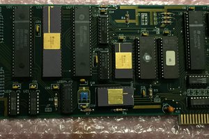
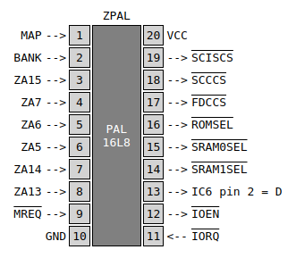
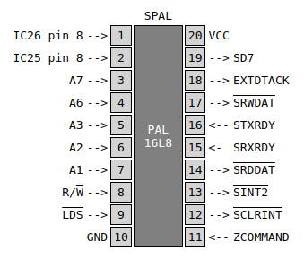
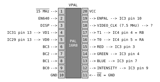
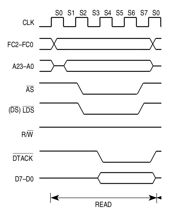
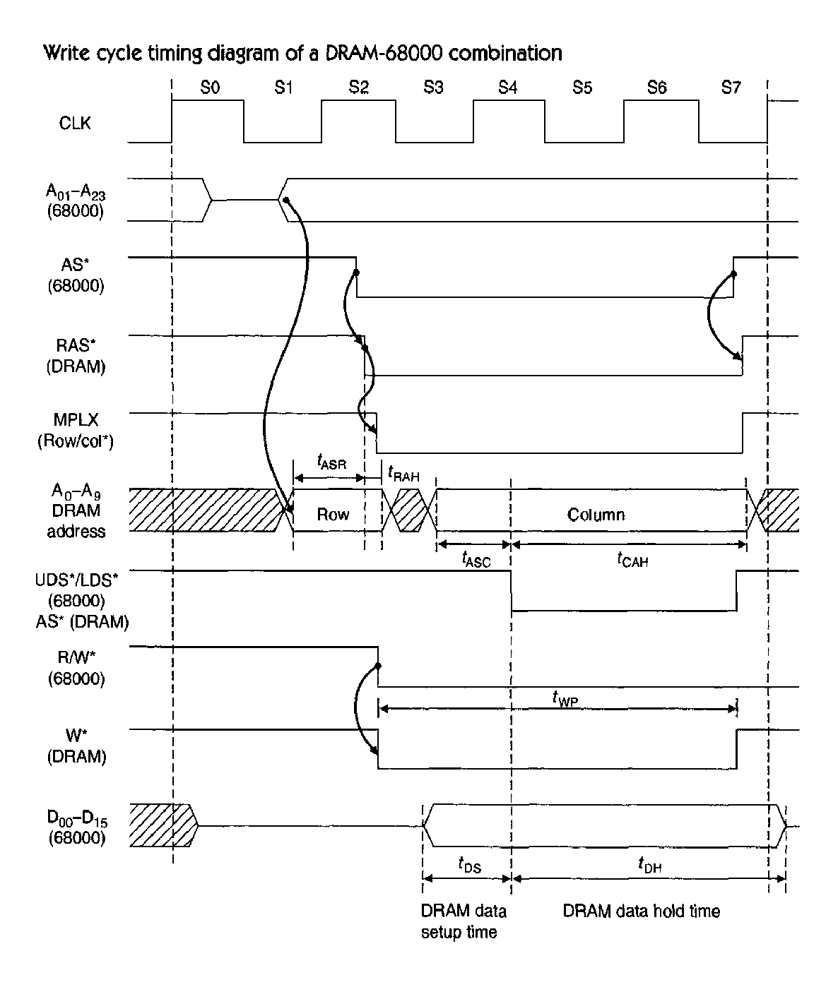
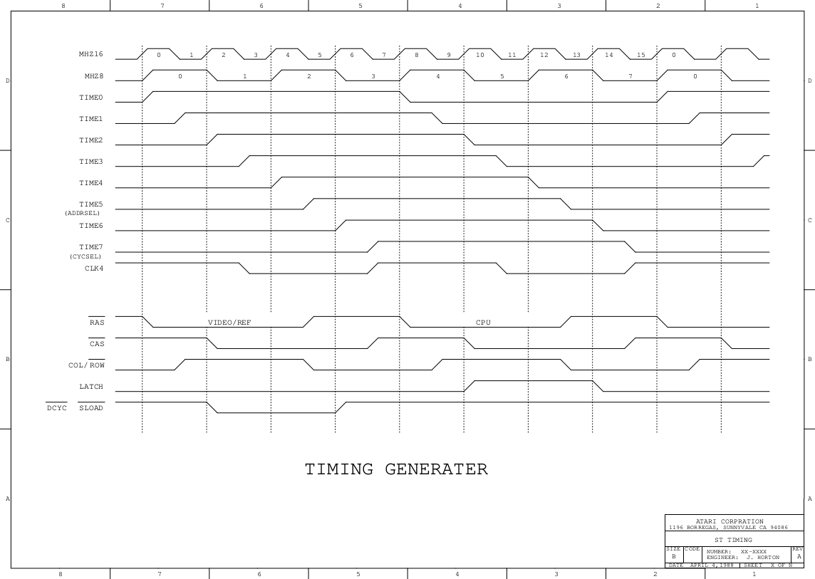
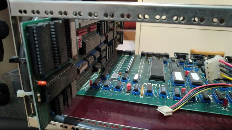
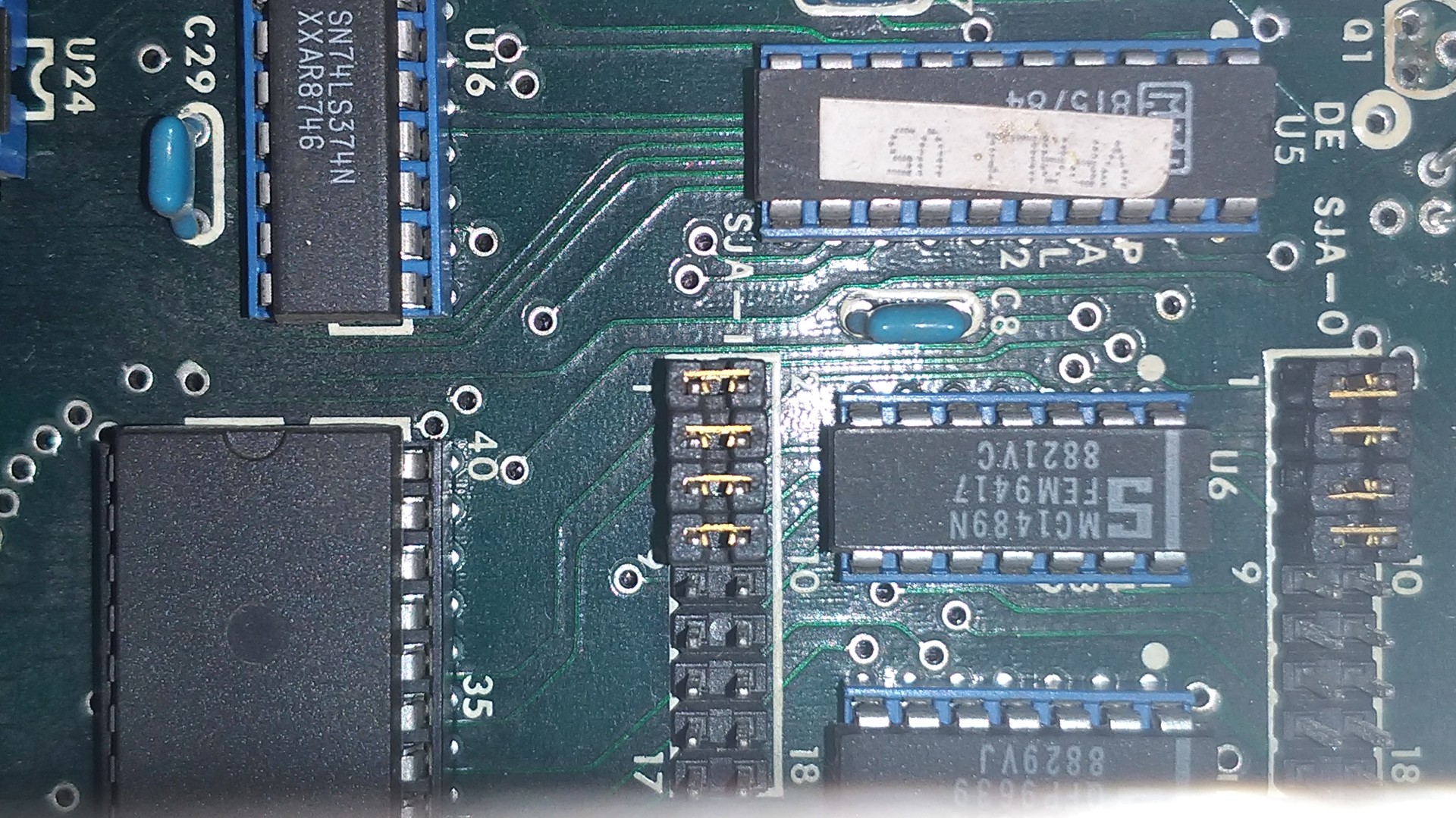
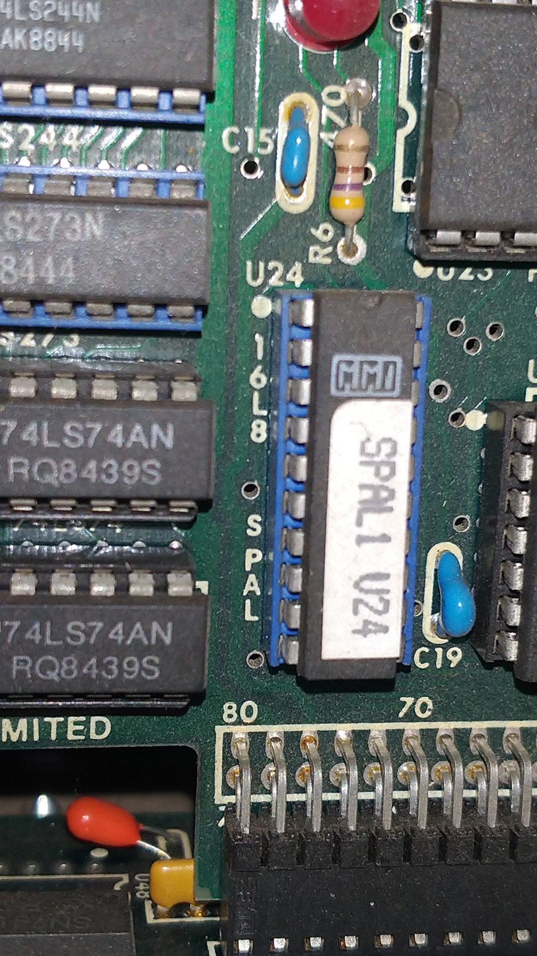
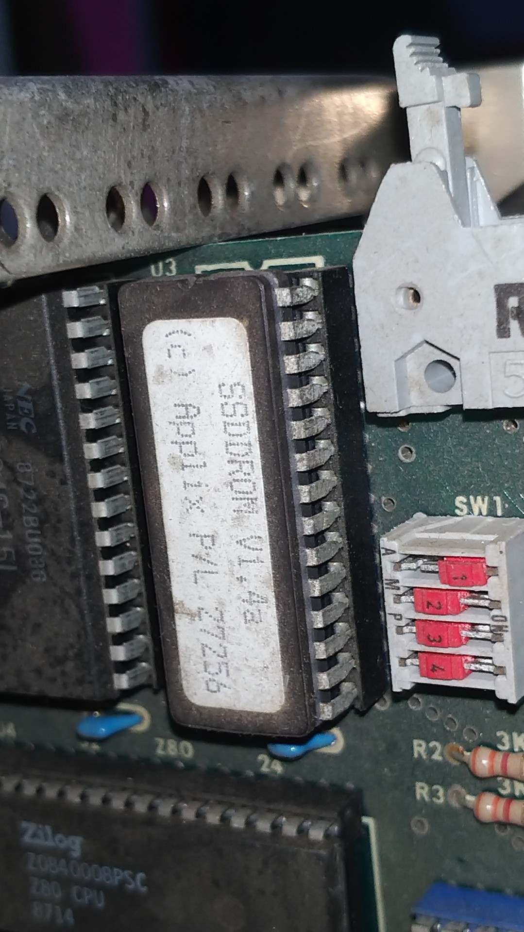
Recreating the PAL devices is my main concern, as they are the only obstacle to recreating the 1616 completely. I have the timing diagrams of an Atari machine, which is a good starting point. Without any information or access to the 1616 chips or waveforms, it is impractical to try cloning them. However, I thought it might be possible to make a primitive 1616 circuit that is just a 68000 (or 68008) chip that runs a loop generating video access DRAM cycles. I have some spare CPUs in my collection. Alternatively I could try creating a model in FPGA.

Atari_timing_from_ASIC_ST4081S_page_7,8,48,49.pdf

Example 68000 cpu/video interleaved DRAM timing diagrams of an Atari ST machine.

Adobe Portable Document Format - 83.02 kB - 11/19/2023 at 01:46

Preview
Download

PAL16L8 ZPAL1 V8.pld.txt

First draft guess at what is going on, from looking at the circuit and the manual. Not tested yet!!!

text/plain - 2.11 kB - 11/01/2023 at 04:41

Download

PAL16L8 SPAL1 V24.pld.txt

First draft guess at what is going on, from looking at the circuit and the manual. Not tested yet!!!

plain - 2.24 kB - 10/29/2023 at 22:36

Download

Applix_programmables.zip

Applix programmable device contents, ROM and PAL. NB the PAL contents are only reading the outputs of the PALs for all possible inputs, which are only an aid to analysis and not a JEDEC programming files.

Zip Archive - 443.23 kB - 10/29/2023 at 14:02

Download

AllPALs.txt

Notes about some PALs. The combinatorial PALs (e.g. 16L8) are read as if they were ROM chips, and the address and data order indicated. There is no equivalent data for the registered PALs.

plain - 1.40 kB - 10/22/2023 at 14:12

Download

View all 10 files

  • 1 × 68000 processor
  • 16 × 41256-15 256 x 1-bit DRAM, 150ns

  • SCSI and Memory board

    Keith11/03/2023 at 03:49 0 comments

    I've looked at this board and there are eight PAL chips, one of which is registered, which I feel is too much effort to reverse engineer for 4 MByte of DRAM and a SCSI interface. It could be largely replaced by eight 512K byte SRAM chips. 

    It uses 256k x 4-bit DRAM, which you can add four at a time. The kind of applications that require a lot of RAM are better served by a modern PC with at least a thousand times more RAM (over 4 GB) and faster with it.

    I read that the SCSI interface is faster to use directly than asking an 8 MHz Z80 slave to do the work. But then it is probably simpler, cheaper and faster to bit-bang an SD card interface. The main reason for a SCSI interface is to extract data from SCSI drives, which are rare and expensive these days.

  • 1617 ZPAL analysis

    Keith10/23/2023 at 23:43 0 comments

    U8 ("ZPAL") - the glue logic for the onboard Z80 microcomputer

    The Z80’s memory map is as follows

    0000H-5FFF H:ROM
    6000H-7FFF Common RAM bank H:
    8000H-FFFF Switching RAM bank H:

    So that the Z80 may access all of the possible 64 kbytes of RAM whilst still reading from the ROM, the RAM is split into two 32k halves. 

    Only one of these halves may appear in the top 32k of address space at a time. When the ‘BANK’ signal is low the data in RAM0 (IC1) is accessible in this address range; when ‘BANK’ is high the data in RAM1 (IC2) is accessible. 

    If 8 kbyte RAM chips are loaded in the board then only the first 8 kbytes of this 32k address space are useful. The first 8 kbytes of RAM is always accessible in the common bank. The ‘MAP’ signal is not used at present.

    The Z80’s I/O port address map is as follows:

    Address Name     Function
    00H     PORT     Read only input port.
    08H     LATCH    Read/write disk select latch
    10H     ZINTS    Write: interrupt the 1616.
    10H     ZCLRINT  Read: clear pending Z80 interrupt.
    18H     SDATA    Read/write 1616 communications port.
    20H     SCSIBASE SCSI controller base address
    40H     FDCBASE  Floppy disk controller base address.
    60H     SCCBASE  Serial communications controller base address.

     The input port enables a Z80 program to determine the level of the following signals:

    Bit 0: The ‘SCOMMAND’ signal is set when the byte from the 1616 which is currently held in the receive latch is a command, meaning that the MC68000 put the data there by writing to its ‘SCOMMAND’ output port.

    Bit 1: The ‘ZRXRDY’ signal is high if there is a data or command byte from the MC68000 within the receive register.

    Bit 2: The ‘ZTXRDY’ signal is high if the 1616 has read the previous byte out of the transmit register.

    Bit 3: This signal determines whether the Z80 is to enter its normal operating mode or to execute its diagnostic test mode.

    Again, does not look difficult.


  • 1617 SPAL analysis

    Keith10/23/2023 at 23:42 0 comments

    U24 ("SPAL") - the expansion bus interface logic

    Pins 1 and 2 go low at the I/O space (A23 to A8 are high). A7-A1, R/W, and /LDS are basic 68000 signals. 

    The manual states that the memory map looks like this:

    $FFFFFC1 R/W    ZDATA     Read:  Data from Z80. 
                              Write: Data to Z80.
    $FFFFC3 Read   SCLRINT    Clear 1616 interrupt.
    $FFFFC3 Write  SINTZ      Interrupt Z80.
    $FFFFC9 Read   SRXRDY     Bit 7 set if receive latch full.
    $FFFFCB Read   STXRDY     Bit 7 set if transmit latch empty.
    $FFFFCD Read   ZCOMMAND   Bit 7 set if contents of the receive latch
                              is a command.   
    $FFFFD1 Write  SCOMMAND   Write data to the data latch,
                              set SCOMMAND bit.

    The PAL multiplexes SRXRDY and STXRDY onto SD7.

    Basically the two processors communicate through two 8-bit latches.

    This all looks pretty simple to implement.

    The binary behaviour data seems wrong, because pin 18 is listed as an input when it should be an output. 

    So I just had a quick go at deducing the logic by reading the manual and the circuit.

  • 1616 VPAL analysis

    Keith10/23/2023 at 23:23 0 comments

    IC5, VPAL, Video

    VIDEO_CLK is simply half the 15 MHz clock frequency. The PAL can work in two modes.

    In 640-pixel wide mode, two bits from the shift registers (VD1, VD0) are fed to T0-1 to drive a 2-bit-address 4-bit-data look-up table, acting as a colour palette.

    In 320-pixel-wide mode, VD1, VD0 are shifted into RED, GREEN, BLUE and INTENSITY. 

    BC0-3 is the Background Colour.

    An LS157 multiplexer (IC3) selects either the RGBI bits from the PAL (IC5) or the palette (IC4). ENPAL selects which.

    I don't think this would be very hard to reverse engineer. The worst case is that wrong colours appear on the screen, which won't harm the 1616 hardware and would usefully indicate what is going wrong.

  • 1616 TPAL analysis

    Keith10/23/2023 at 23:20 0 comments

    IC15, TPAL, Timing PAL

    We can see that pins 19,18,17 are a simple clocked counter. Other signals control DRAM, and other designs might provide a starting model. The RAM is interleaved VDU/CPU access, so the DRAM signals may only begin just after the VDU phase has finished.

    I suspect that this forms a state machine with 8 states per memory cycle, and generates a fixed sequence of DRAM access signals from those states. Which makes sense, because the 6845 does not do that. I also suspect it generates the same sequence for CPU access, but simply making the CPU wait until it is complete.

    Scoping the signals would give a good idea of the DRAM signals to be created.

    Alternatively, you might be able to tell the PAL it is doing video cycles, and then record the state of the output pins as it is clocked. Pins 17, 18 and 19 are going to cycle through states 0 to 7, and the DRAM control signals should change at the same states throughout an 8-state memory cycle.

    It is worth noting that the microprocessors of the 1980s all ran at pretty much the same memory cycle rate. A 1 MHz 6502 had 1 clock per memory cycle, a 4 MHz Z80 had 3 or 4 clocks per memory cycle, and an 8 MHz 68000 had 8 clocks per memory cycle. All of these would have around the same 1 MHz memory cycle rate.

    If you get the DRAM signals wrong, the computer will crash straight away, so I doubt it would have time to do any damage to the 1616. You could make a small gadget that turns off the 1616 if does not run some code that disables the gadget in time. This would prevent the 1616 running for any significant length of time with a non-valid DRAM interface.

    The 68000 memory read cycle

    ... looks like this:

    So I would expect a /RAS signal to be similar to /AS, with /CASU and /CASL to resemble /UDS and /LDS respectively.

    The DRAM control signals will be a function of the signals on pins 17 to 19.

    To find the timing, one would have to tell the PAL it is in video cycles (using DISPEN?) and then toggle the clock (pin1) and record the state of the outputs as they cycle through eight states.

    This can be done at human speed, just by applying a debounced pulse on pin 1.

    Until that gets done, I will look for existing 68000 DRAM interfaces. This is hard to find, as it is not the sort of thing people tackled unless they were a big company. However, I did find a book that covered the subject in great detail: 
    68000 hardware, software, and interfacing by Allan Clements.
    After much text about DRAM in general, it presents a 68000 to DRAM timing diagram on page 390:

    This provides a good starting point where there is only one DRAM access per CPU cycle. /AS is effectively /RAS and /DS is effectively /CAS. 

    For interleaved video/CPU access, the CPU DRAM access must be crammed into the second half (S4-7) and the video access crammed into the first half (S0-3).

    Example timings are hard to find. This sort of thing goes on in the 1616, the Apple Mac, the Atari ST, the Commodore Amiga, The Sinclair QL.... but manufacturers were not keen on disclosing such details.

    I eventually found some timings from some files salvaged from Atari after they went bust. Here is the timing of one of their chips:

    For the 1616, the signals "MHZ16" and "MHZ8" would be the 15 and 7.5 MHz clocks respectively.

    The MHZ8 signal has the numbers 0 to 7, representing the 68000 CPU states S0 to S7.

    The Atari ASIC derives timings by shifting a 2 MHz square wave through an 8-bit shift register at 32 MHz. This makes it easy to decode timings with very little logic. For instance:

    /SLOAD =  TIME2 * /TIME6 ; /* a NAND and NOT gate for single pulse */
    LATCH  = /TIME2 *  TIME6 ;
    /RAS   =  TIME0 * /TIME5 + /TIME0 * TIME5 ; /* a XOR gate for double pulses */
    COL    =  TIME1 * /TIME5 + /TIME1 * TIME5 ; 
    /CAS   =  TIME2 * /TIME7 + /TIME2 * TIME7 ;
    CLK4   = /TIME3 * /TIME7 +  TIME3 * TIME7 ;

     The 1616 TPAL derives timings by using its 30 and 15 MHz inputs and a 3-bit synchronous...

    Read more »

  • 1617 PAL reverse engineering

    Keith10/22/2023 at 18:06 0 comments

    The 1617 is a SCSI and Floppy drive controller board.

    Fortunately the PAL chips are purely combinatorial PAL16L8. 

    Their output patterns have been read.

  • 1616 PAL reverse engineering

    Keith10/22/2023 at 00:17 0 comments

    These devices are the only things standing in the way of the 1616 being a fully open source design.

    Alas they had their security bits programmed, and the designers have lost the original source files.

    From the circuit diagram, we can read the functions and the signal directions.

    ChipTester V2 Pro says it analyses registered PAL chips. Yes it does, but only in the same way as it analyses combinatorial chips. Cefiar's binary files have 256 identical bytes, which suggests it did not do any clocking at all. The results are effectively useless.

    What is needed

    ... is a gadget to apply clocked test sequences and examine the results. If one knows nothing about a PAL, one has to apply very many test sequences and a great deal of analysis. I think I recall someone trying to do this with a fairly powerful microcontroller, and eventually concluding it would need something based on an FPGA to do it fast enough.

    If one knows something about the PAL, such as the input and output pin functions, one can make intelligent guesses and cut down the work greatly.

    Parallel testing

    One way to test if two chips work the same (without damaging the host board) is to run them in parallel with the same input signals, and then compare their output signals. This requires building a PCB that holds both chips and plugs into the original socket. Comparison can be done visually by comparing scope traces, or XOR gates. The latter will have many fine glitches but at least show how much outputs differ.

    This will be a slow process if PALs are shipped from the UK to Australia.

    An alternative is to ship a GAL programmer and email test patterns for the recipient to program and test.

  • Stuart's system

    Keith10/21/2023 at 15:06 0 comments

    Stuart is restoring a 1616 machine and documenting his progress at:

    https://forum.acms.org.au/t/retrochallenge-2023-10-applix1616-restoration-documentation/503/4

    He has read the PAL chips using a ChipTester V2 Pro from BackBit.io and I eagerly await looking at them. I don't know whether the security bits were blown or not. If they were, one can only make a best guess by examining the behaviour. 

    There is a project that tries to dump PAL contents. Easily done for combinatorial chips, less so for registered chips. 

    See: https://github.com/DuPAL-PAL-DUmper

    I don't know how clever it is, or how reliable the output.

    Worst case, I could make a best guess replacement and ask Cefiar to try them out.

    His system has:

    • 1616 processor motherboard
    • SCSI and Memory Expansion board
    • Two intelligent Z80-based Floppy Disc Controller boards

    Both SCSI and floppy discs are obsolete, and I am not very motivated to reverse engineer the PALs although they should be fairly simple to do.

    The motherboard PALs are registered and harder to reverse engineer. I can't scope his system (and nor can he) but I think I could make a good guess at the 68000 DRAM interface by scoping my Atari ST here.

  • Andrew's system

    Keith10/02/2023 at 01:11 0 comments

View all 9 project logs

Enjoy this project?

Share

Discussions

Similar Projects

Does this project spark your interest?

Become a member to follow this project and never miss any updates